Self-aligned bipolar semiconductor device and fabrication method thereof

a bipolar semiconductor and fabrication method technology, applied in the field of self-aligned bipolar semiconductor devices and fabrication methods thereof, can solve problems such as not only solving problems, current gain is not reduced, and base resistance is decreased

Inactive Publication Date: 2006-07-06
DONGBU ELECTRONICS CO LTD
View PDF2 Cites 11 Cited by
  • Summary
  • Abstract
  • Description
  • Claims
  • Application Information

AI Technical Summary

Problems solved by technology

Furthermore, in SiGe HBT devices, current gain is not reduced and base resistance is decreased even if impurity concentration is increased.
This may not only solve problems due to mask misalignment, but also reduce device size.
The selective growth of the epitaxial layer is, however, susceptible to quality and shape of a fundamental substrate.
Furthermore, since the epitaxial layer grows isotropically, the growth of the epitaxial layer may invite electrical short-circuit between adjacent devices.
This may unfavorably induce complex processes, a reduction in active regions due to bird's beak, variation of impurity concentration due to lengthy thermal process, an increase in leakage current due to stress occurring in selective oxidation.

Method used


Image

  • Self-aligned bipolar semiconductor device and fabrication method thereof
  • Self-aligned bipolar semiconductor device and fabrication method thereof
  • Self-aligned bipolar semiconductor device and fabrication method thereof

Examples


Embodiment Construction

[0028] An exemplary, non-limiting embodiment of the present invention will now be described more fully hereinafter with reference to the accompanying drawings. This invention can, however, be embodied in many different forms and should not be construed as limited to the exemplary embodiment set forth herein. Rather, the disclosed embodiment is provided so that this disclosure will be thorough and complete, and will fully convey the disclosure of the invention to those skilled in the art. The principles and features of this invention can be employed in varied and numerous embodiments without departing from the scope of the invention.

[0029] In is noted that well-known structures and processes are not described or illustrated in detail to avoid obscuring the essence of the present invention. It is also noted that the figures are not drawn to scale.

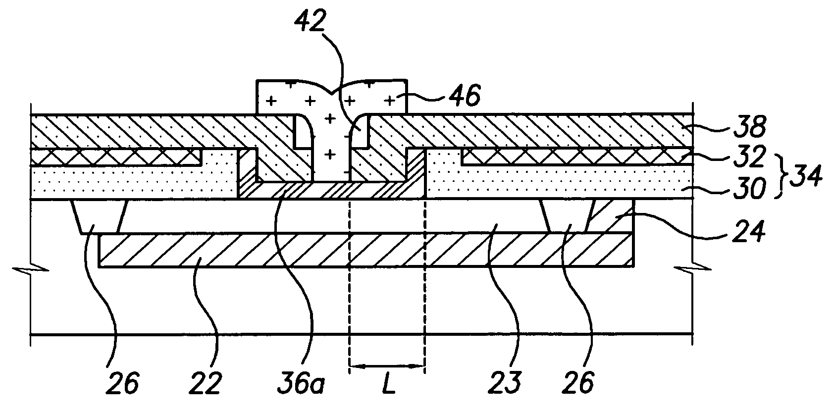
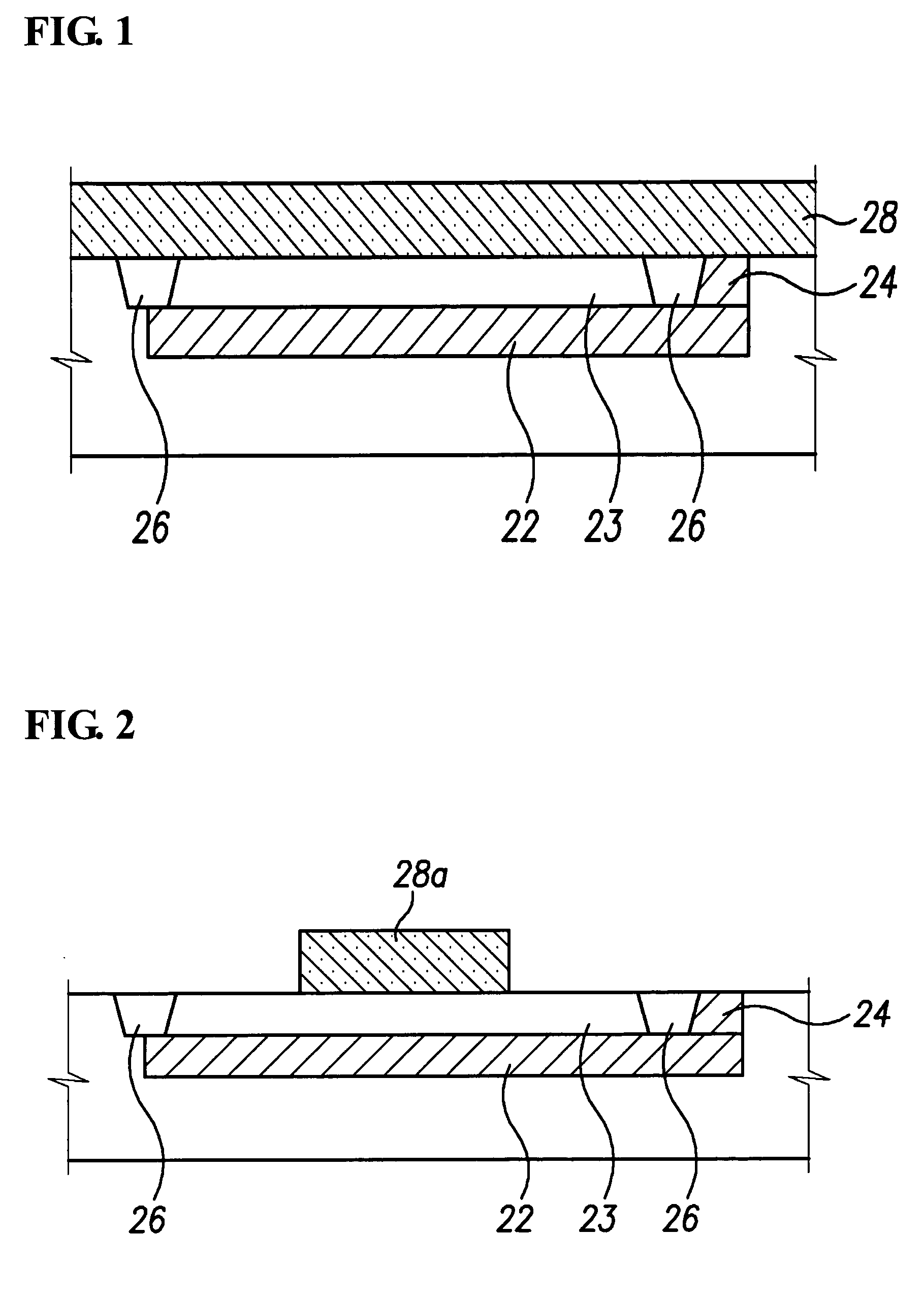
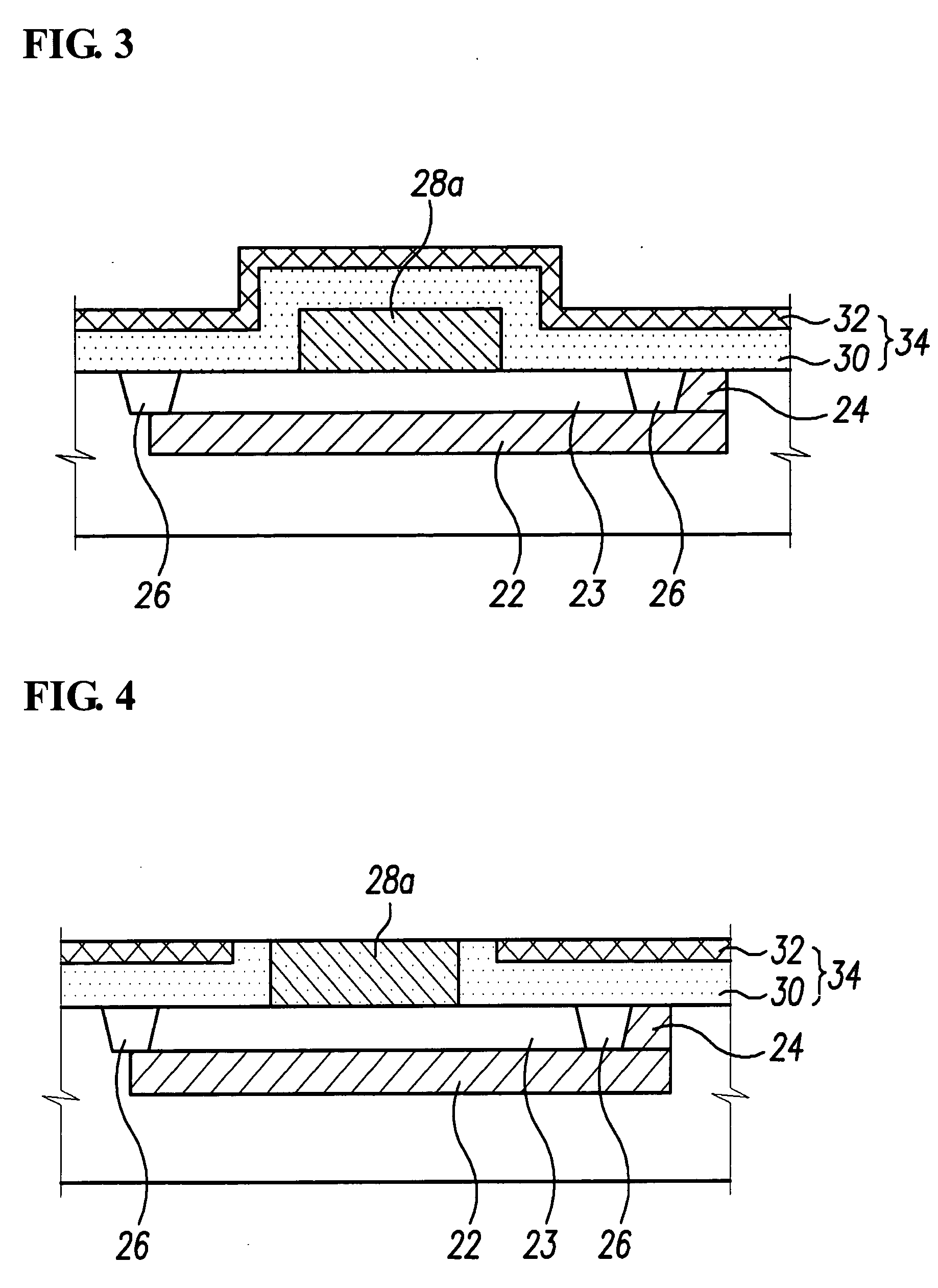
[0030] FIGS. 1 to 8 are cross-sectional views showing a method of fabricating a self-aligned bipolar semiconductor device in accordance wi...


PUM


Abstract

A self-aligned bipolar semiconductor device and a fabrication method thereof are provided. After a silicon layer and a collector contact are formed on a buried collector layer, an oxide dummy pattern is formed on the silicon layer to define both an extrinsic base and an intrinsic base. A polycide layer used as the extrinsic base is formed thereon and selectively removed to expose the dummy pattern. After the exposed dummy pattern is removed, an epitaxial layer used as the intrinsic base is grown on both the silicon layer and the polycide layer, and selectively removed from the top of the polycide layer. An oxide layer and a nitride layer are deposited in sequence thereon, and the nitride layer is blanket-etched to form spacers defining an emitter. After a photoresist pattern is formed to mostly cover the oxide layer and partly expose the oxide layer between the spacers over the intrinsic base, the oxide layer is etched by using the photoresist pattern and the spacers as an etch mask.

Description

CROSS REFERENCE TO RELATED APPLICATIONS [0001] This U.S. non-provisional application claims priority under 35 U.S.C. §119 from Korean Patent Application No. 2004-117847, which was filed in the Korean Intellectual Property Office on Dec. 31, 2004, the contents of which are incorporated by reference herein in its entirety. BACKGROUND OF THE INVENTION [0002] 1. Field of the Invention [0003] The present invention relates generally to semiconductor integrated circuit (IC) technology and, more particularly, to a self-aligned bipolar semiconductor device and a fabrication method thereof. [0004] 2. Description of the Related Art [0005] In comparison with typical MOS (metal oxide semiconductor) devices, BJT (bipolar junction transistor) devices have some advantages of relatively better current performance and higher operating speed. Hence the use of BJT devices is on an increasing trend in various branches of semiconductor IC technologies. [0006] Additionally, HBT (heterojunction bipolar tra...

Claims


Application Information

Patent Timeline
Patent Type & Authority Applications(United States)
IPC IPC(8): H01L21/331H01L21/8222
CPCH01L29/0821H01L29/66287H01L29/732H01L29/737
Inventor YOON, YEO CHO
Owner DONGBU ELECTRONICS CO LTD
Why Eureka
Try Eureka