Method for manufacturing semiconductor device

a semiconductor and manufacturing technology, applied in the direction of semiconductor devices, basic electric elements, electrical appliances, etc., can solve the problems of reducing yield, reducing the possibility of chipping at division and subsequent chipping of semiconductor devices, and reducing the possibility of product whose semiconductor substrate is chipped, etc., to achieve the effect of reducing the possibility of chipping at division and subsequent to the completion of a semiconductor devi

Inactive Publication Date: 2006-07-13
LAPIS SEMICON CO LTD
View PDF8 Cites 28 Cited by
  • Summary
  • Abstract
  • Description
  • Claims
  • Application Information

AI Technical Summary

Benefits of technology

[0016] According to the present invention, the possibility that chipping at division and chipping subsequent to the completion of

Problems solved by technology

In the CSP type semiconductor device, however, there have been known so-called chipping problems that when a semiconductor wafer is divided into fractions or pieces, a semiconductor substrate is get chipped, and the semiconductor substrate is chipped upon handling of the semiconductor wafer subsequent to being divided into the pieces and completed as each of the semiconductor devices (the former will hereinafter be called “chipping at division” and the latter will hereinafter be called “chipping subsequent to completion of each semiconductor device”).
Therefore, chipping is visually recognized even after the completion of the semiconductor device when the chipping occurs in the semiconductor substrate (around the outer edge portion of the back in particular) even at the division, thus reducing yields.
Even though a semiconductor device that

Method used


Image

  • Method for manufacturing semiconductor device
  • Method for manufacturing semiconductor device
  • Method for manufacturing semiconductor device

Examples


first preferred embodiment

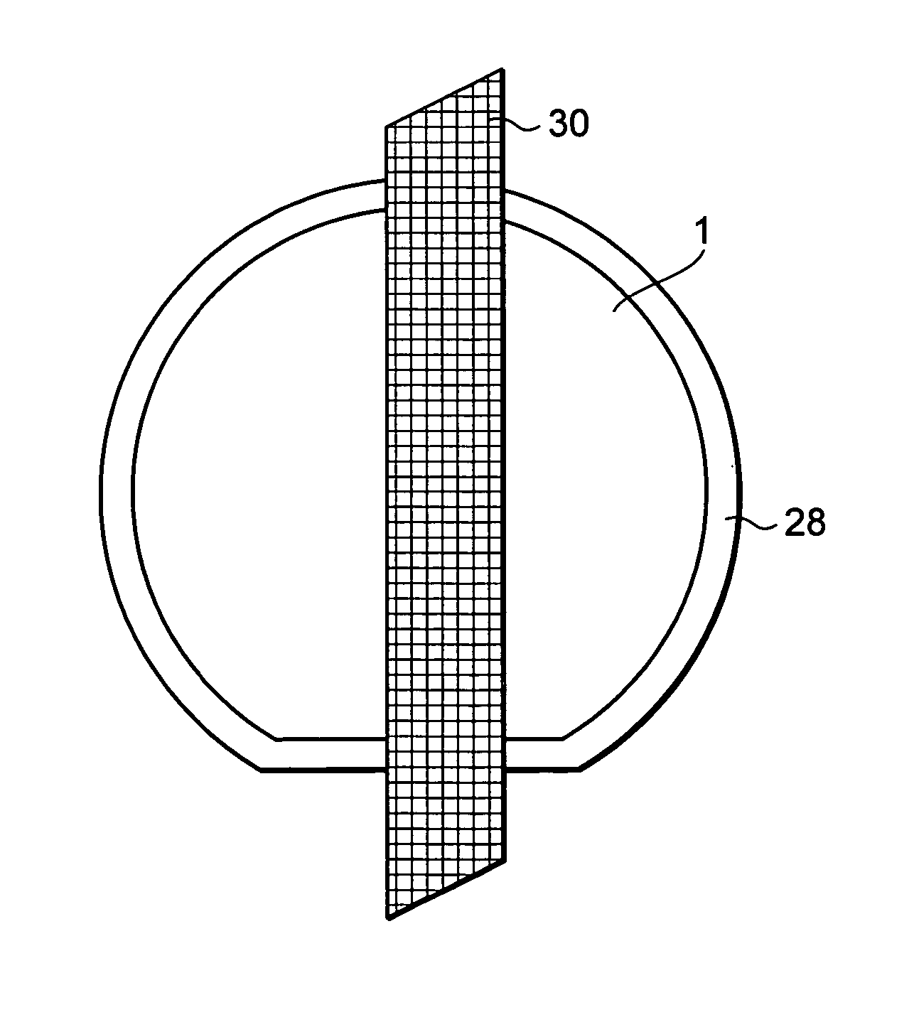
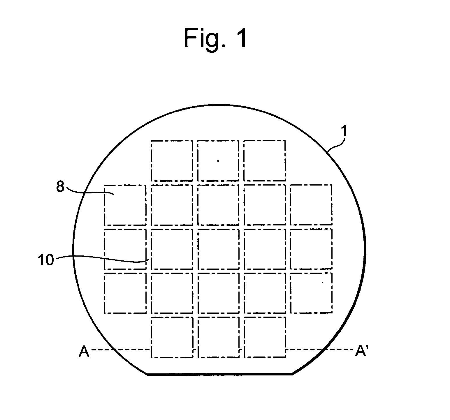
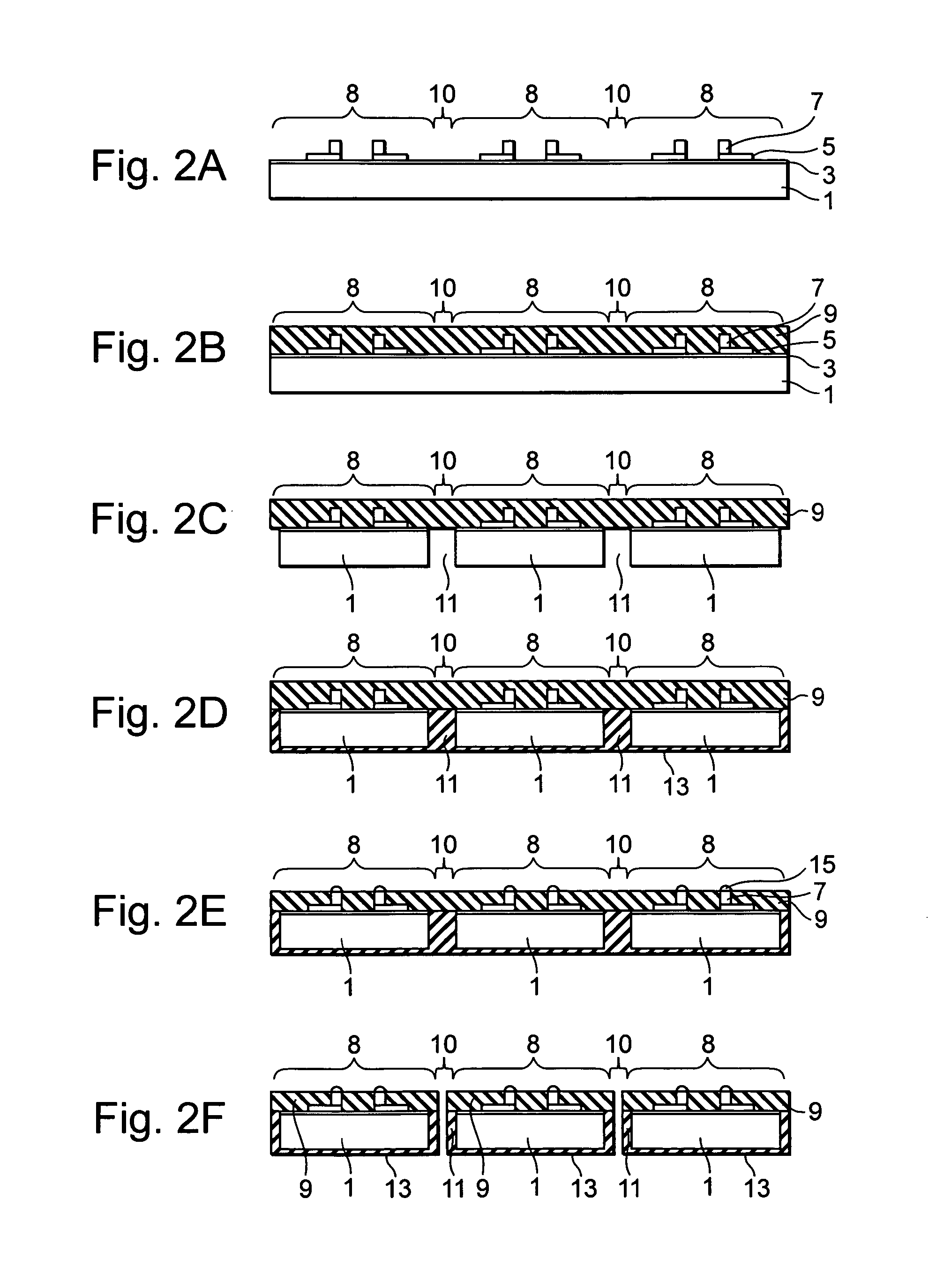
[0030] A method for manufacturing a semiconductor device, according to a first embodiment of the present invention will be explained using FIGS. 1 through 4. FIG. 1 is a plan view of a semiconductor wafer of the present embodiment, and FIGS. 2(A) through 2(F) are respectively sections taken every manufacturing process steps in the present embodiment and sectional views each showing a portion taken along line A-A′ of FIG. 1. FIG. 3 is a view showing, in an enlarged form, a sectional view illustrating a trench forming process step [process step 1-3]. FIG. 4 is a sectional view of a semiconductor device manufactured by the manufacturing method of the present embodiment.

[Process Step 1-1] Protruded Electrode Forming Step:

[0031] As shown in FIGS. 1 and 2(A), posts 7 (protruded electrodes) are first respectively formed on a plurality of chip areas 8 of a semiconductor wafer 1 having the plurality of chip areas 8 and boundary regions 10 formed among the chip areas 8 both of which are pr...

second preferred embodiment

[0060] A method for manufacturing a semiconductor device, according to a second embodiment of the present invention will be explained with reference to FIG. 1, FIG. 5 and FIG. 6. FIG. 1 is a plan view of a semiconductor wafer employed in the present embodiment. FIGS. 5(A) through 5(F) are sections taken every manufacturing process steps in the semiconductor device manufacturing method according to the second embodiment and are sectional views taken along line A-A′ of FIG. 1. FIG. 6 is a sectional and bottom view of a semiconductor device manufactured by such a manufacturing method.

[Process Step 2-1] Protruded Electrode Forming Step:

[0061] As shown in FIGS. 1 and 5(A), posts 7 (protruded electrodes) are first respectively formed on a plurality of chip areas 8 of a semiconductor wafer 1 having the plurality of chip areas 8 and boundary regions 10 formed among the chip areas 8 both of which are provided in the surface of the semiconductor wafer 1. That is, the semiconductor wafer 1 ...


PUM


Abstract

A method for manufacturing a semiconductor device comprises the steps of forming protruded electrodes on a plurality chip areas of a semiconductor wafer having the plurality of chip areas and boundary regions formed among the chip areas, both being provided in a surface of the semiconductor wafer, forming a surface-side protective member so as to cover the surface of the semiconductor wafer and the protruded electrodes, removing the semiconductor wafer corresponding to the boundary regions and forming trenches which expose the surface-side protective member, forming a back-side protective member with which the trenches are filled and which covers the back of the semiconductor wafer, and dividing the semiconductor wafer in the boundary regions with widths thinner than those of the trenches in such a manner that the surface-side protective member and the back-side protective member charged into the trenches are left in cut sections.

Description

FIELD OF THE INVENTION [0001] The present invention relates to a method for manufacturing a semiconductor device of a chip size package (also called a chip scale package, which will hereinafter be called “CSP”) type assembled in a package substantially identical in dimension to a semiconductor chip. BACKGROUND OF THE INVENTION [0002] There has recently been a strong demand for reductions in the size and thickness of an integrated circuit package in which semiconductor integrated circuits have been packaged. In response to such a demand, a CSP type semiconductor device is known wherein external connecting solder bumps are provided within a semiconductor chip size to attain its size reduction. [0003] In the CSP type semiconductor device, however, there have been known so-called chipping problems that when a semiconductor wafer is divided into fractions or pieces, a semiconductor substrate is get chipped, and the semiconductor substrate is chipped upon handling of the semiconductor waf...

Claims


Application Information

Patent Timeline
IPC IPC(8): H01L21/78H01L21/301
CPCH01L21/78H01L2224/96
Inventor KUSHIMA, YOSHIMASAYAMAGUCHI, TADASHI
Owner LAPIS SEMICON CO LTD
Why Eureka
Try Eureka