
Substrate processing apparatus using a batch processing chamber

a processing apparatus and batch technology, applied in the direction of coatings, chemical vapor deposition coatings, metallic material coating processes, etc., can solve the problems of increasing coo, affecting the final product quality,

Inactive Publication Date: 2006-07-20
APPLIED MATERIALS INC
View PDF56 Cites 364 Cited by
  • Summary
  • Abstract
  • Description
  • Claims
  • Application Information

AI Technical Summary

Benefits of technology

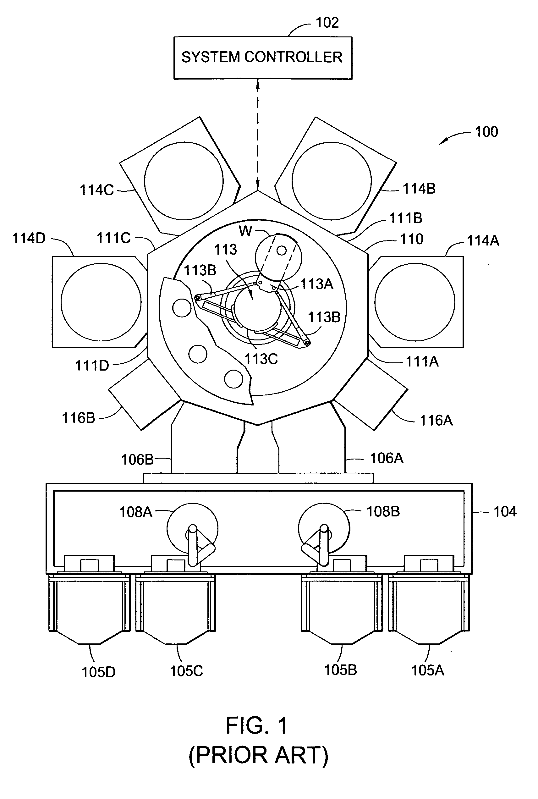
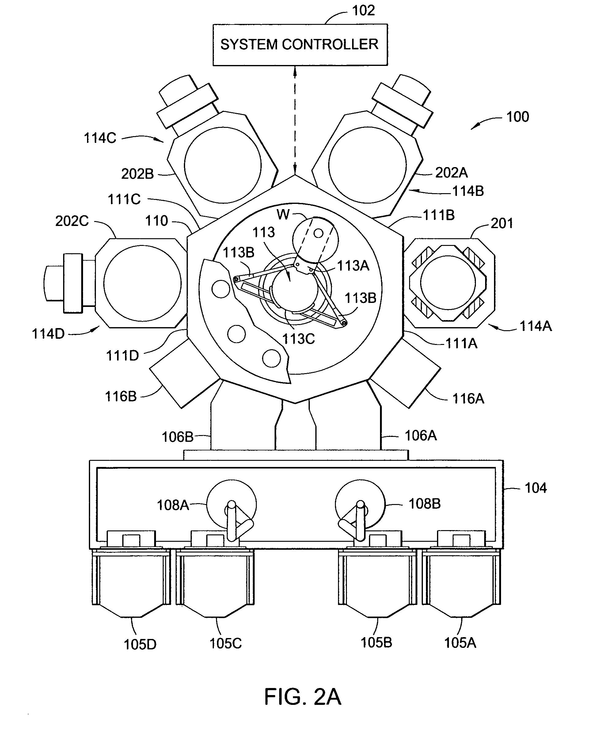
[0057] Embodiments of the invention have particular advantages in a cluster tool which has the capability to process substrates in single substrate processing chambers and batch type processing chambers. A cluster tool is a modular system comprising multiple chambers which perform various functions in the electronic device fabrication process. As shown in FIG. 1, the multiple chambers are mounted to a central transfer chamber 110 which houses a robot 113 adapted to shuttle substrates between the chambers. The transfer chamber 110 is typically maintained at a vacuum condition and provides an intermediate stage for shuttling substrates from one chamber to another and / or to a load lock chamber positioned at a front end of the cluster tool.

Problems solved by technology

If the substrate throughput in a cluster tool is not robot limited, the longest process recipe step will generally limit the throughput of the processing sequence, increase the COO and possibly make a desirable processing sequence impractical.
To meet these tighter process requirements, the industry has developed a host of new processes which meet the tighter process window requirements, but these processes often take a longer time to complete.
While forced to choose such processes due to device performance requirements, the cost to fabricate the devices in a conventional single substrate processing chamber will increase due to the low substrate throughput.
Also, while it is possible to add more tools to the wafer fab to meet the desired number of wafer starts per week (or substrate starts per week), it is often impractical to increase the number of process chambers or tools without significantly increasing the size of a wafer fab and the staff to run the tools, because these are often the most expensive aspects of the substrate fabrication process.
Due to the shrinking size of semiconductor devices and the ever increasing device performance requirements, the amount of allowable variability of the device fabrication process uniformity and repeatability has greatly decreased.
If the substrate is exposed to atmospheric or other sources of contaminants for a time approaching or longer than the allowable queue time, the device performance may be affected by the contamination of the interface between the first and second layers.

Method used


Image

  • Substrate processing apparatus using a batch processing chamber
  • Substrate processing apparatus using a batch processing chamber
  • Substrate processing apparatus using a batch processing chamber

Examples


Embodiment Construction

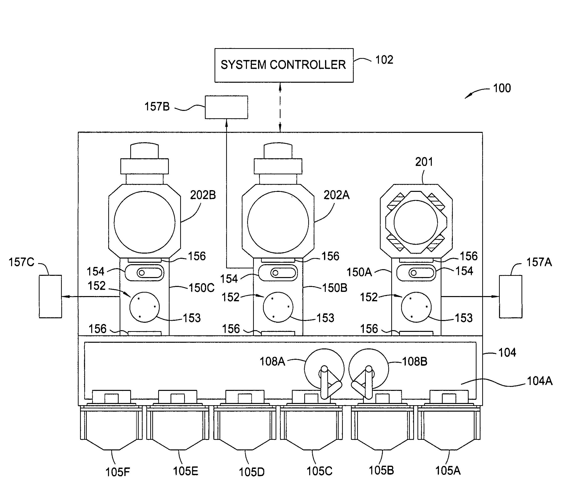
[0056] The present invention generally provides an apparatus and method for processing substrates using a multi-chamber processing system (e.g., a cluster tool) adapted to process substrates in one or more batch and single substrate processing chambers to increase the system throughput. The term batch processing chamber, or batch capable processing chamber, is meant to generally describe a chamber that can process two or more substrates at one time. In one embodiment, a batch processing chamber is used to increase the system throughput by performing a process recipe step that is disproportionately long compared to other process recipe steps in the substrate processing sequence that are performed on the cluster tool. In another embodiment, two or more batch chambers are used to process multiple substrates using one or more of the disproportionately long processing steps in a processing sequence. In one aspect of the invention, a system controller is utilized to control the number of ...


PUM

PropertyMeasurementUnit
pressureaaaaaaaaaa
atmospheric pressureaaaaaaaaaa
temperatureaaaaaaaaaa

Abstract

Aspects of the invention include a method and apparatus for processing a substrate using a multi-chamber processing system (e.g., a cluster tool) adapted to process substrates in one or more batch and / or single substrate processing chambers to increase the system throughput. In one embodiment, a system is configured to perform a substrate processing sequence that contains batch processing chambers only, or batch and single substrate processing chambers, to optimize throughput and minimize processing defects due to exposure to a contaminating environment. In one embodiment, a batch processing chamber is used to increase the system throughput by performing a process recipe step that is disproportionately long compared to other process recipe steps in the substrate processing sequence that are performed on the cluster tool. In another embodiment, two or more batch chambers are used to process multiple substrates using one or more of the disproportionately long processing steps in a processing sequence. Aspects of the invention also include an apparatus and method for delivering a precursor to a processing chamber so that a repeatable ALD or CVD deposition process can be performed.

Description

CROSS-REFERENCE TO RELATED APPLICATIONS [0001] This application claims benefit of U.S. Provisional Patent Application Ser. No. 60 / 630,501, filed Nov. 22, 2004, and U.S. Provisional Patent Application Ser. No. 60 / 642,877, filed Jan. 10, 2005, which are both herein incorporated by reference.BACKGROUND OF THE INVENTION [0002] 1. Field of the Invention [0003] Embodiments of the invention generally relates to an integrated processing system configured to perform processing sequences which include both single substrate and batch deposition processing modules. [0004] 2. Description of the Related Art [0005] The process of forming semiconductor device is commonly done in a multi-chamber processing system (e.g., a cluster tool) which has the capability to process substrates, (e.g., semiconductor wafers) in a controlled processing environment. A typical controlled processing environment will include a vacuum system that has a mainframe which houses a substrate transfer robot which transports ...

Claims


Application Information

Patent Timeline
Patent Type & Authority Applications(United States)
IPC IPC(8): H01L21/322C23C16/00
CPCC23C16/45546C23C16/45593C23C16/4584C23C16/481C23C16/54H01L21/67017H01L21/67109H01L21/67115H01L21/67167H01L21/6719H01L21/67207H01L21/67745H01L21/67757H01L21/67781C23C16/4412C23C16/00H01L21/306
Inventor THAKUR, RANDHIRGHANAYEM, STEVE G.YUDOVSKY, JOSEPHWEBB, AARONBRAILOVE, ADAM ALEXANDERMERRY, NIRSHAH, VINAY K.HEGEDUS, ANDREAS G.
Owner APPLIED MATERIALS INC
Learn More