

Structure and method to optimize strain in cmosfets
- Summary
- Abstract
- Description
- Claims
- Application Information
AI Technical Summary
Benefits of technology
Problems solved by technology
Method used
Image

Examples
Embodiment Construction
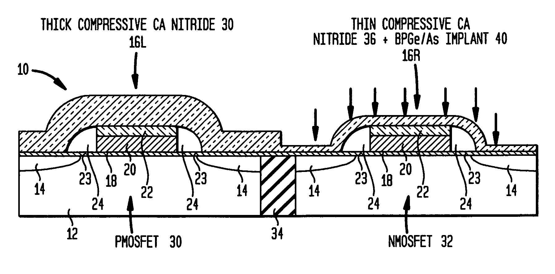
[0009] The present invention provides a MOSFET structure with different thicknesses of contact barrier (CA) nitride on NMOSFETs and PMOSFETs that maximizes the strain in one type / kind (P or N) of MOSFET and minimizes and relaxes the strain in another type / kind (Nor P) of MOSFET.
[0010]FIG. 1 illustrates first and second exemplary embodiments of the present invention on a semiconductor wafer having both PMOSFETs 30 and NMOSFETs 32 separated by isolation regions 34. In the first and second exemplary embodiments of the present invention, compressive CA nitride is used to maximize the strain in the PMOSFETs 30 and minimize and relax the strain in the NMOSFETs 32.
[0011] In summary, after deposition of a thick (700-1000 A) compressive CA nitride 36 on both the PMOSFETs 30 and the NMOSFETs 32, the wafer is patterned with photoresist such that the PMOSFETs 30 are covered by photoresist and the NMOSFETs 32 are exposed and not covered by photoresist. The CA nitride at the NMOSFETs 32 is etch...
PUM
 Abstract
Description
Claims
Application Information