

Solid state imaging device and fabrication method thereof, and camera incorporating the solid state imaging device
a technology of solid state imaging and fabrication method, which is applied in the direction of instruments, television systems, and television system scanning details, etc., can solve the problems of difficult material selection, difficult formation of light-shielding black film pattern by lithography, and restricted photosensitive resists. , to achieve the effect of simplifying the fabrication process
- Summary
- Abstract
- Description
- Claims
- Application Information
AI Technical Summary
Benefits of technology
Problems solved by technology
Method used
Image

Examples
embodiment 1
[0061] Hereinafter, a solid state imaging device according to embodiment 1 of the present invention is described. It should be noted that a CCD solid state imaging device is herein described as an example, but the present invention is not limited thereto. For example, the present invention is applicable to a MOS solid state imaging device, and the like.
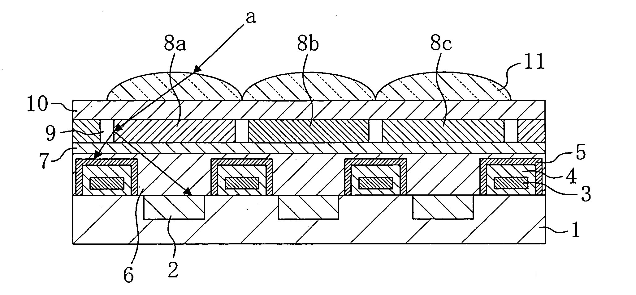
[0062]FIG. 1 is a cross-sectional view showing a structure of a solid state imaging device according to embodiment 1. As shown in FIG. 1, the solid state imaging device of embodiment 1 includes a semiconductor substrate 1, a plurality of light receiving sections 2 arranged in a matrix over the semiconductor substrate 1, transfer electrodes 3 provided on the semiconductor substrate 1 in regions between the light receiving sections 2.
[0063] The transfer electrodes 3 are provided over the semiconductor substrate 1 with the intervention of a dielectric film 4. Over the transfer electrodes 3 and the dielectric film 4 is a light shielding...
embodiment 2
[0068] Hereinafter, a solid state imaging device according to embodiment 2 of the present invention is described. It should be noted that a CCD solid state imaging device is herein described as an example, but the present invention is not limited thereto. For example, the present invention is applicable to a MOS solid state imaging device, and the like.
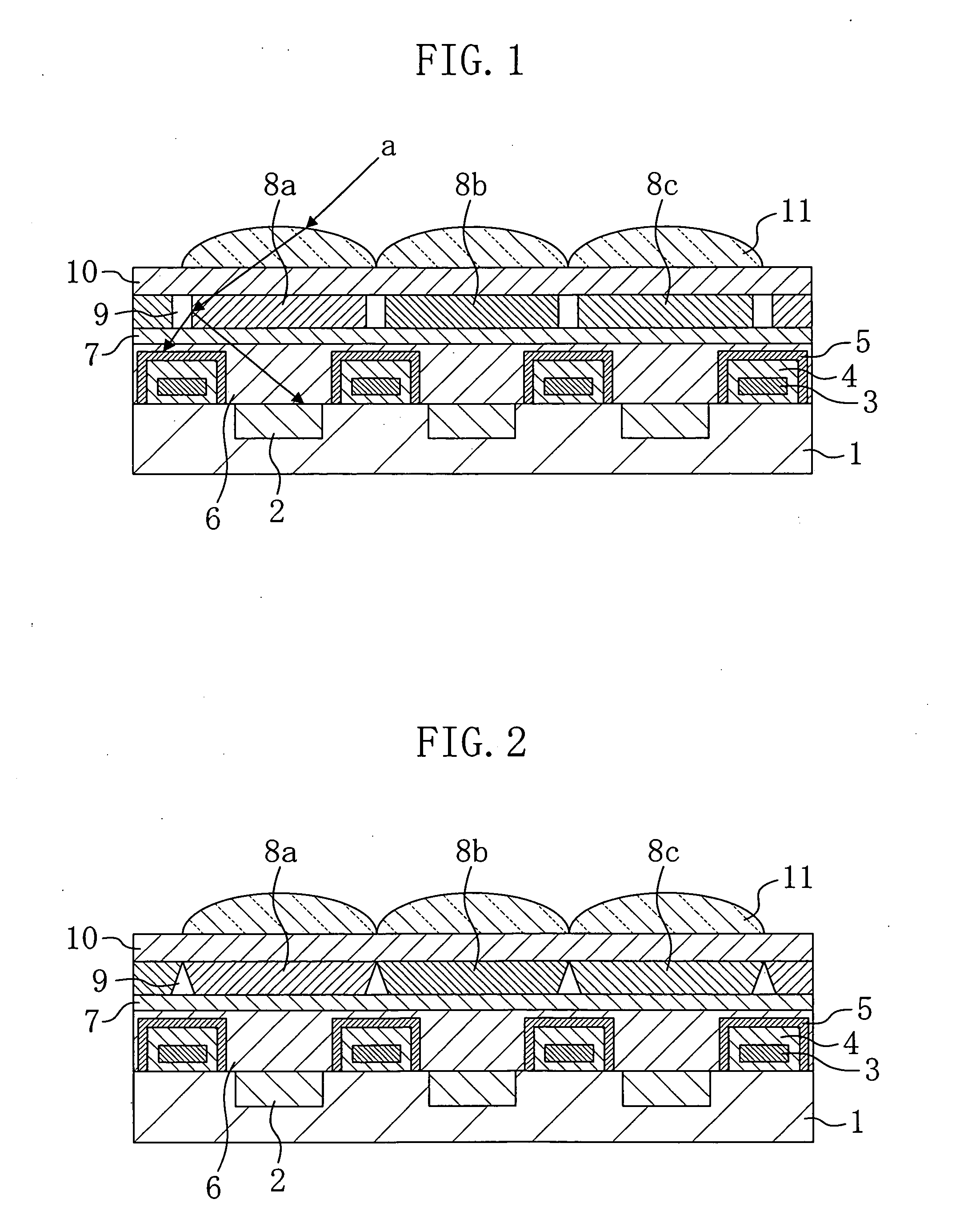
[0069]FIG. 3 is a cross-sectional view showing a structure of the solid state imaging device according to embodiment 2. As shown in FIG. 3, the solid state imaging device of embodiment 2 includes a semiconductor substrate 1, a plurality of light receiving sections 2 arranged in a matrix over the semiconductor substrate 1, transfer electrodes 3 provided on the semiconductor substrate 1 in regions between the light receiving sections 2.
[0070] The transfer electrodes 3 are provided over the semiconductor substrate 1 with the intervention of a dielectric film 4. Over the transfer electrodes 3 and the dielectric film 4 is a light shieldi...
embodiment 3
[0074] Hereinafter, a solid state imaging device according to embodiment 3. of the present invention is described. It should be noted that a CCD solid state imaging device is herein described as an example, but the present invention is not limited thereto. For example, the present invention is applicable to a MOS solid state imaging device, and the like.
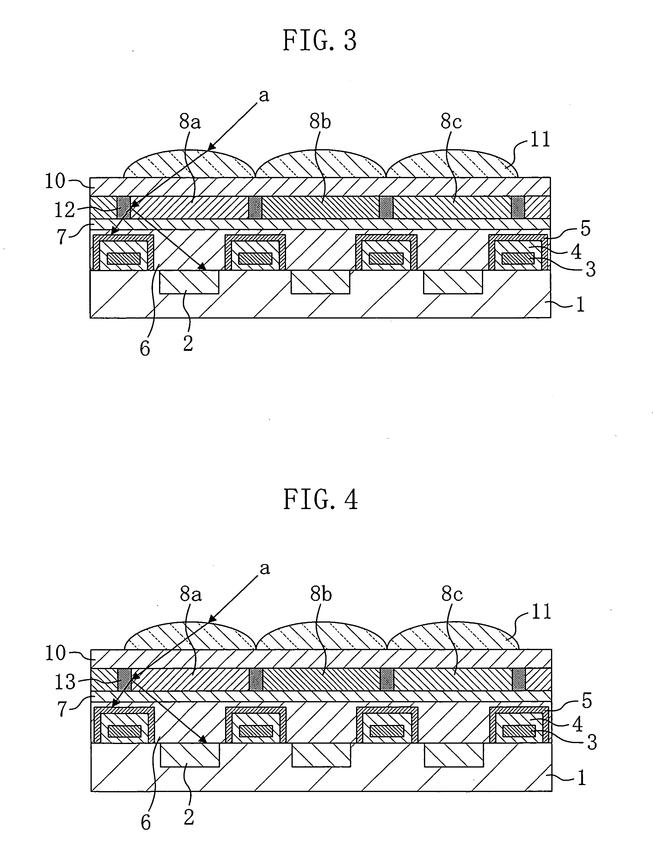
[0075]FIG. 4 is a cross-sectional view showing a structure of the solid state imaging device according to embodiment 3. As shown in FIG. 4, the solid state imaging device of embodiment 3 includes a semiconductor substrate 1, a plurality of light receiving sections 2 arranged in a matrix over the semiconductor substrate 1, transfer electrodes 3 provided on the semiconductor substrate 1 in regions between the light receiving sections 2.
[0076] The transfer electrodes 3 are provided over the semiconductor substrate 1 with the intervention of a dielectric film 4. Over the transfer electrodes 3 and the dielectric film 4 is a light shield...
PUM
 Abstract
Description
Claims
Application Information