

Switching regulator circuit
- Summary
- Abstract
- Description
- Claims
- Application Information
AI Technical Summary
Benefits of technology
Problems solved by technology
Method used
Image

Examples
first embodiment
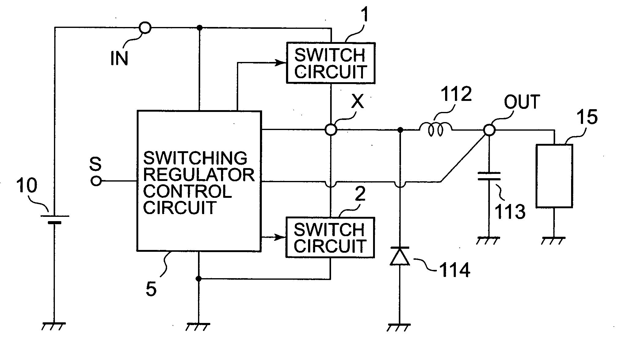
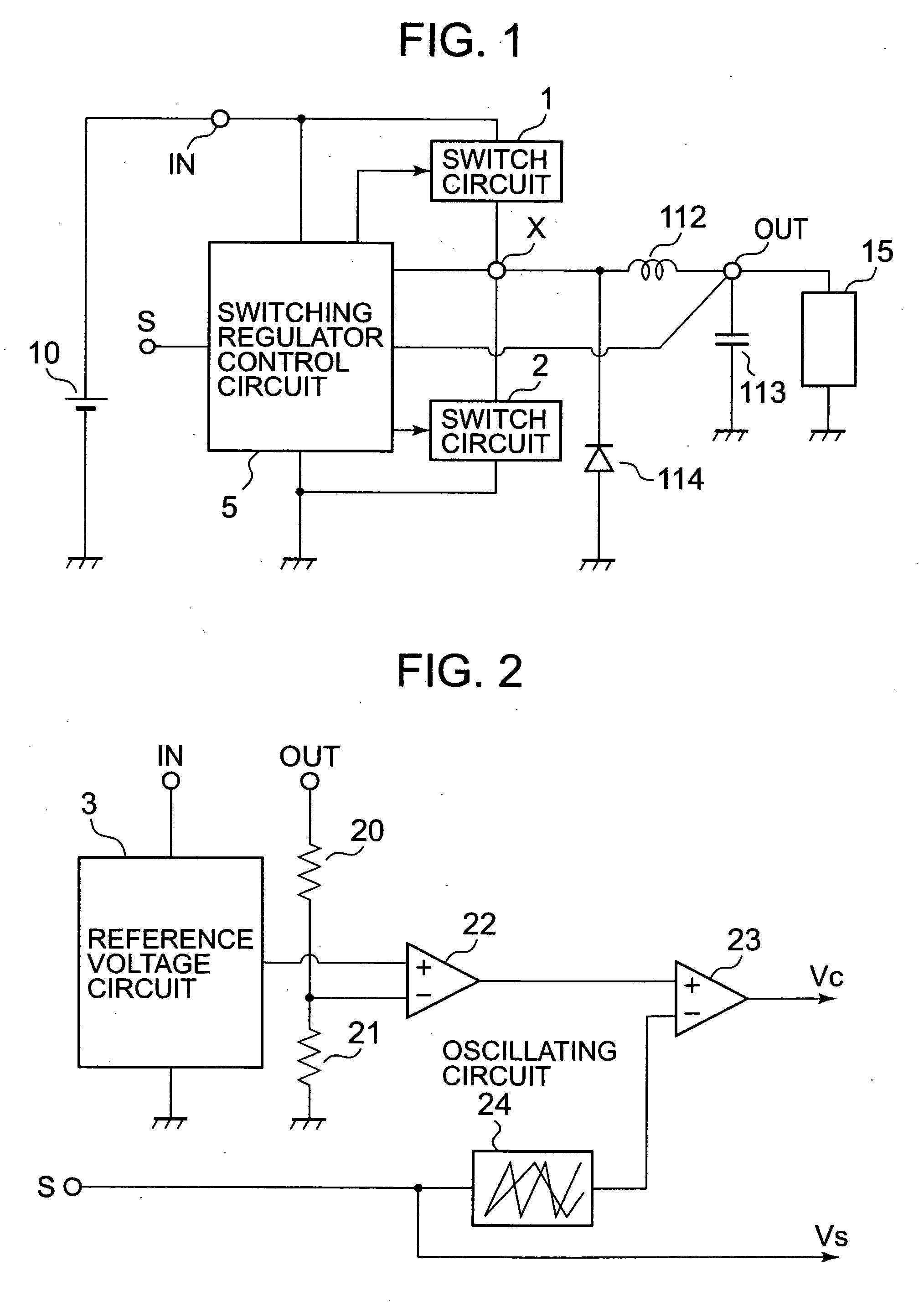
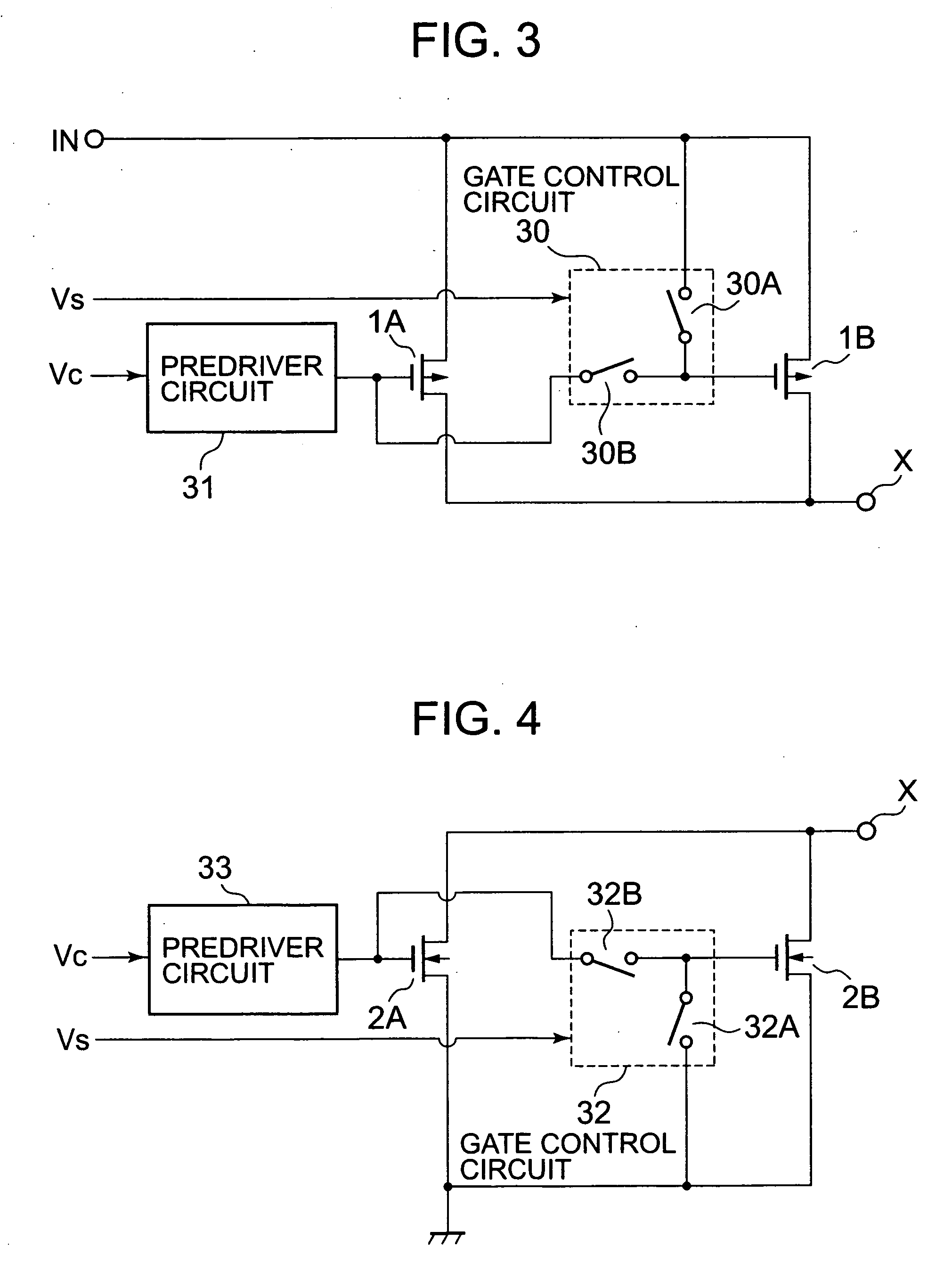
[0040] Hereinafter, embodiments of the present invention will be described based on the drawings. FIG. 1 shows a switching regulator according to a first embodiment of the present invention. The difference from the conventional example of FIG. 16 resides in that a switching regulator control circuit 5 includes an input terminal S for an input from outside. A first switch circuit 1 including a switch element and a second switch circuit 2 including a switch element change drive capabilities of the respective switch elements based on a signal from the switching regulator control circuit 5. Further, when an oscillating frequency inside the switching regulator control circuit 5 changes based on a voltage of the input terminal S, the drive capabilities of the first and second switch elements 1 and 2 change simultaneously.
[0041]FIG. 2 is a block diagram of the switching regulator control circuit 5 of the present invention. A reference voltage circuit 3 outputs a constant voltage. A dividi...
second embodiment
[0059]FIG. 6 is a block diagram of the switch circuit 1 of the switching regulator according to a second embodiment of the present invention.
[0060] The difference from FIG. 3 resides in that predriver circuits 41 and 42 exist instead of the predriver circuit 31 and the gate control circuit 30 is deleted. The predriver circuit is a circuit for driving switch elements. To drive a large-scale switch element, a predriver circuit assumedly needs to have high drive capability. In general, the higher the drive capability is, the lager the switching loss is. The predriver circuit 41 is a circuit for driving the MOS transistor 1A and the predriver circuit 42 is a circuit for driving the MOS transistor 1B. Similar to FIG. 3, the MOS transistors 1A and 1B have different drive capabilities, namely, ON resistances. When the ON resistance of the MOS transistor 1A is R1A and the ON resistance of the MOS transistor 1B is R1B, the expression (1) is satisfied. Therefore, the switching loss of the pr...
third embodiment
[0066]FIG. 10 shows a switching regulator according to a third embodiment of the present invention. The difference from FIG. 1 resides in that the input terminal S is omitted and a current sense resistor 60 is added between the coil 112 and the output terminal OUT. Signals at both ends of the current sense resistor are connected to a switching regulator control circuit 61. In the switching regulator control circuit 61, as shown in FIG. 11, an amplifying circuit 62 amplifies a voltage of the ends of the resistance. The voltage is compared with that of a reference voltage circuit 64 at a comparator 63. An output of the comparator is set as the signal Vs, which is the input from outside in FIG. 1. Thus, when the load current is large, an output of the amplifying circuit 62 increases, and when the load current is small, the output of the amplifying circuit 62 decreases. When the load current is equal to or lower than a certain value, the output of the comparator 63, namely, Vs, is “L” l...
PUM
 Abstract
Description
Claims
Application Information