Light-emitting element array chip, light-emitting device, optical device, and information processing device
Pending Publication Date: 2021-10-14
FUJIFILM BUSINESS INNOVATION CORP
View PDF0 Cites 0 Cited by
Summary
Abstract
Description
Claims
Application Information
AI Technical Summary
This helps you quickly interpret patents by identifying the three key elements:
Problems solved by technology
Method used
Benefits of technology
[0005]Incidentally, in a light-emitting element array, from a viewpoint of improving power conversion efficiency, there is a method in which a lowe
Problems solved by technology
However, aspects of the non-limiting embodiments are not required to address the advantages described above, an
Method used
Image
Click on the blue label to locate the original text in one second.
Reading with bidirectional positioning of images and text.
Examples
Example
FIRST EXEMPLARY EMBODIMENT
Information Processing Device 1
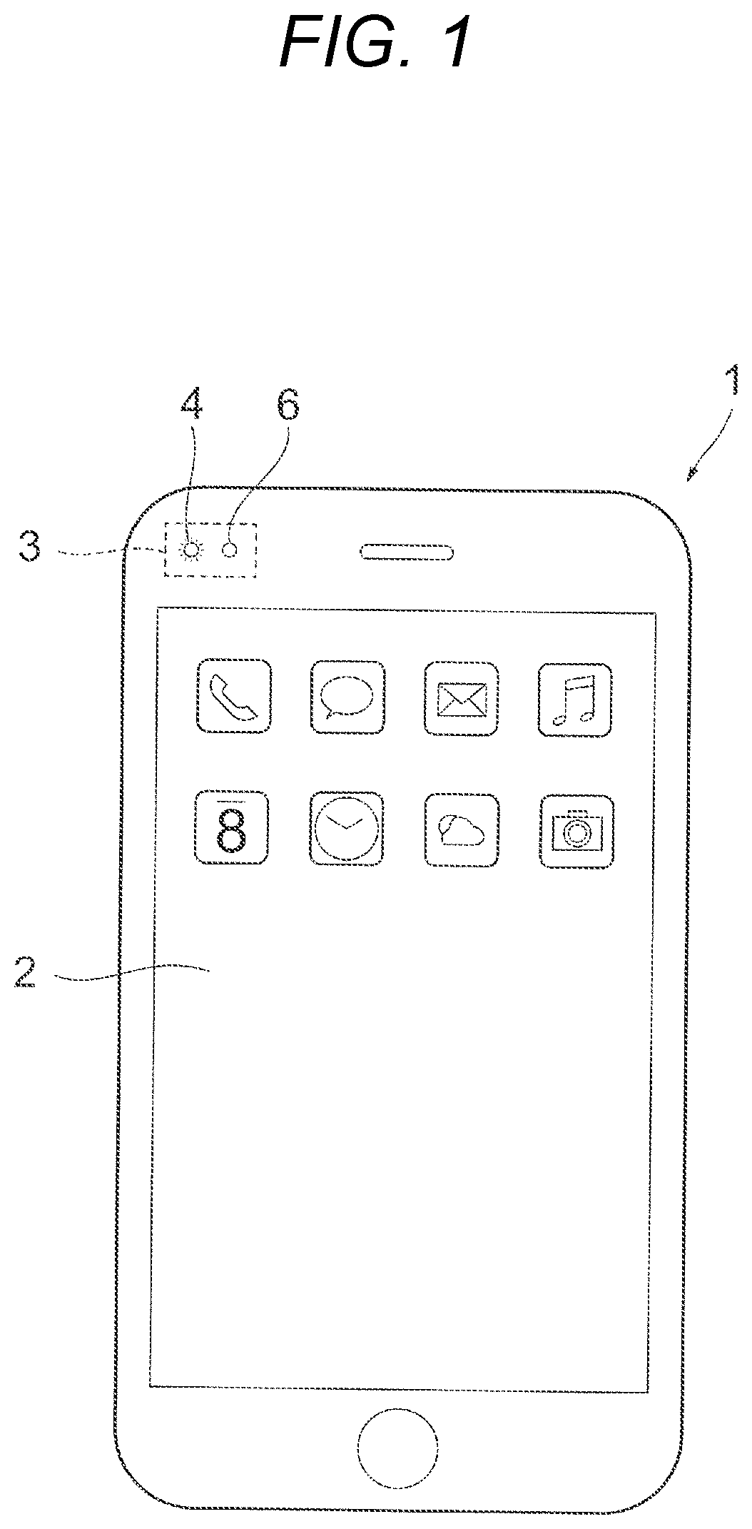
[0032]FIG. 1 is a diagram showing an example of the information processing device 1. As described above, the information processing device 1 is, for example, the portable information processing terminal.
[0033]The information processing device 1 includes a user interface unit (hereinafter, referred to as UI unit) 2 and an optical device 3 that acquires a three-dimensional image. The UI unit 2 is configured by integrating, for example, a display device that displays information to the user and an input device to which an instruction for information processing is input by an operation of the user. The display device is, for example, a liquid crystal display or an organic EL display. The input device is, for example, a touch panel.
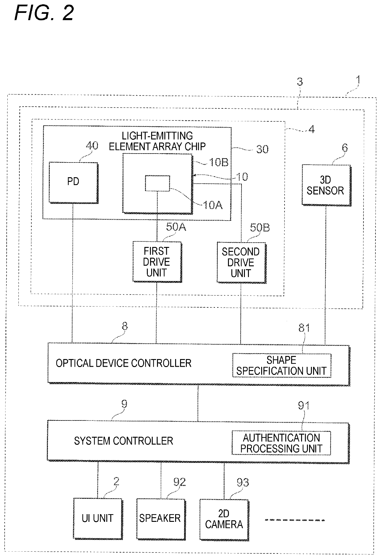
[0034]The optical device 3 includes a light-emitting device 4 and a three-dimensional sensor (hereinafter, referred to as a 3D sensor) 6. The light-emitting device 4 emits light toward the object to be m...
Example
SECOND EXEMPLARY EMBODIMENT
[0115]In the first exemplary embodiment, the VCSEL-B of the high-power light-emitting element array 10B uses the n-type lower DBR 202. In a second exemplary embodiment, a VCSEL-C that constitutes the high-power light-emitting element array 10B uses an i-type (intrinsic) lower DBR 302. That is, in the second exemplary embodiment, the VCSEL-C is used instead of the VCSEL-B. Since other configurations of the second exemplary embodiment are similar to those of the first exemplary embodiment, description thereof will be omitted.
VCSEL-C of High-Power Light-Emitting Element Array 10B
[0116]FIG. 11 is a diagram illustrating a cross-sectional structure of one VCSEL-C of the high-power light-emitting element array 10B to which the second exemplary embodiment is applied.
[0117]In the VCSEL-C, an undoped i-type lower DBR 302 in which undoped i-type AlGaAs layers having different Al compositions are alternately laminated is provided on a semi-insulating i-type GaAs subst...
PUM
Abstract
A light-emitting element array chip includes: a first light-emitting element array that includes a first light-emitting element including a first substrate, a light-emitting element layer formed on the first substrate, and a first cathode electrode electrically connected to the light-emitting element layer; and a second light-emitting element array that includes a second light-emitting element including a second substrate, a non-p-type lower reflector formed on the second substrate, and a second cathode electrode electrically connected to the non-p-type lower reflector, in which the first light-emitting element array is provided on an emission surface side of the second light-emitting element array.
Description
CROSS-REFERENCE TO RELATED APPLICATIONS[0001]This is a continuation of International Application No. PCT / JP2019 / 26709 filed on Jul. 4, 2019, and claims priority from Japanese Patent Application No. 2019-056926 filed on Mar. 25, 2019.BACKGROUNDTechnical Field[0002]The present invention relates to a light-emitting element array chip, a light-emitting device, an optical device, and an information processing device.Related Art[0003]JP-T-2016-507167 discloses a laser diode drive system including a first high-side drive current source for driving a first set of diodes including one or more laser diodes, a second high-side drive current source for driving a second set of diodes including one or more laser diodes, an energy storage capacitor, and an energy storage capacitor charger for charging the energy storage capacitor.[0004]US Patent Publication 10135222 discloses a VCSEL array in which a VCSEL array is divided into plural regions so that the farther the distance to a target object is,...
Claims
Application Information
Patent Timeline
Application Date:The date an application was filed.
Publication Date:The date a patent or application was officially published.
First Publication Date:The earliest publication date of a patent with the same application number.
Issue Date:Publication date of the patent grant document.
PCT Entry Date:The Entry date of PCT National Phase.
Estimated Expiry Date:The statutory expiry date of a patent right according to the Patent Law, and it is the longest term of protection that the patent right can achieve without the termination of the patent right due to other reasons(Term extension factor has been taken into account ).
Invalid Date:Actual expiry date is based on effective date or publication date of legal transaction data of invalid patent.