Epitaxial growth method

a growth method and growth method technology, applied in the field of epitaxial growth method, can solve the problems of high cost, complex anodization method, and many crystalline defects, and achieve the effect of easy formation of a porous buffer layer and low cos

Inactive Publication Date: 2006-07-20
SAMSUNG CORNING PRECISION MATERIALS CO LTD
View PDF9 Cites 19 Cited by
  • Summary
  • Abstract
  • Description
  • Claims
  • Application Information

AI Technical Summary

Benefits of technology

[0008] The present invention provides a method of forming a semiconductor crystalline layer at low cost by easily forming a porous buffer layer.

Problems solved by technology

A substrate on which an epitaxial layer is formed using an epitaxial growth method may be bent and many crystalline defects may arise in the epitaxial layer due to lattice mismatch and a difference in coefficient of thermal expansion between the substrate and the epitaxial layer.
However, since the porous buffer layer is formed using an anodization process, a conductive substrate should be employed, thus only limited kinds of materials may be used for the substrate.
Also, the anodization method is very complicated and costly.

Method used


Image

  • Epitaxial growth method
  • Epitaxial growth method
  • Epitaxial growth method

Examples


Embodiment Construction

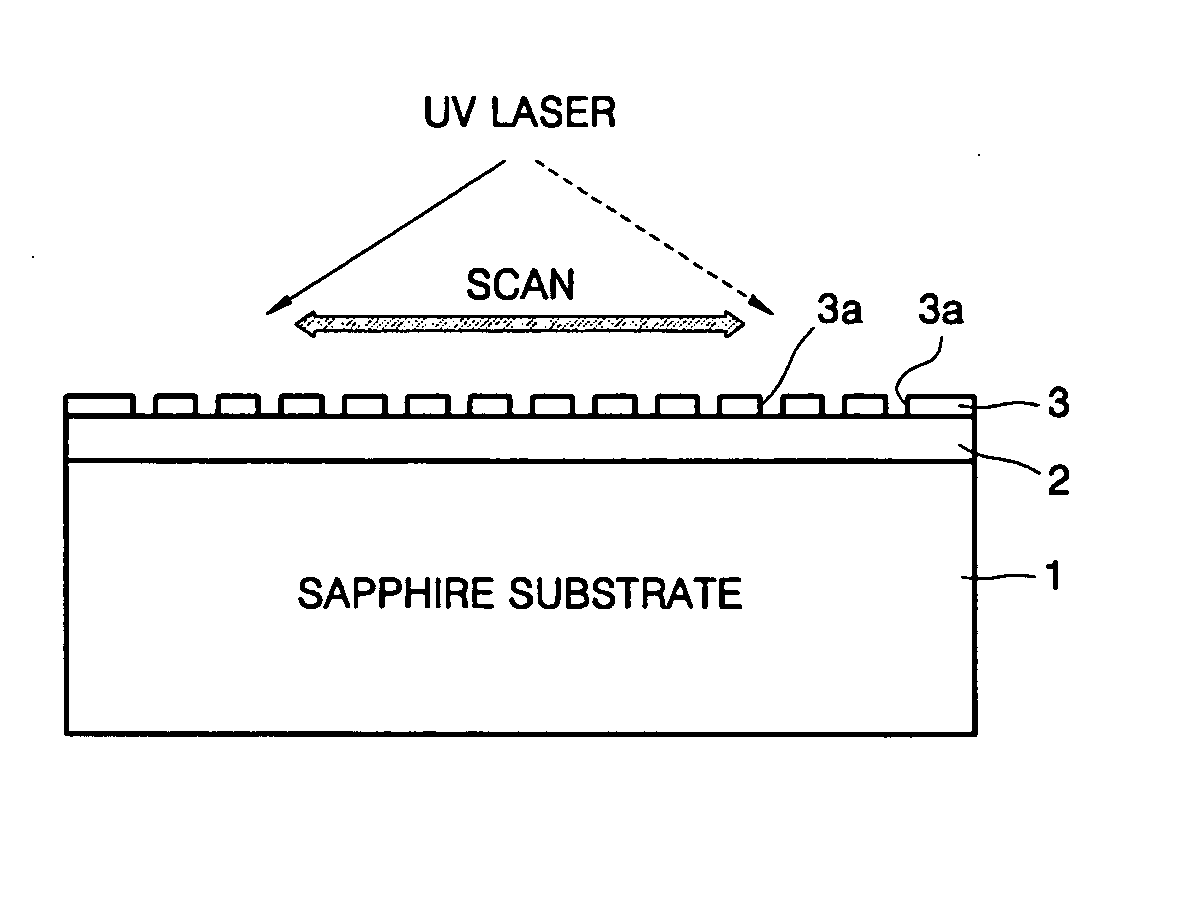
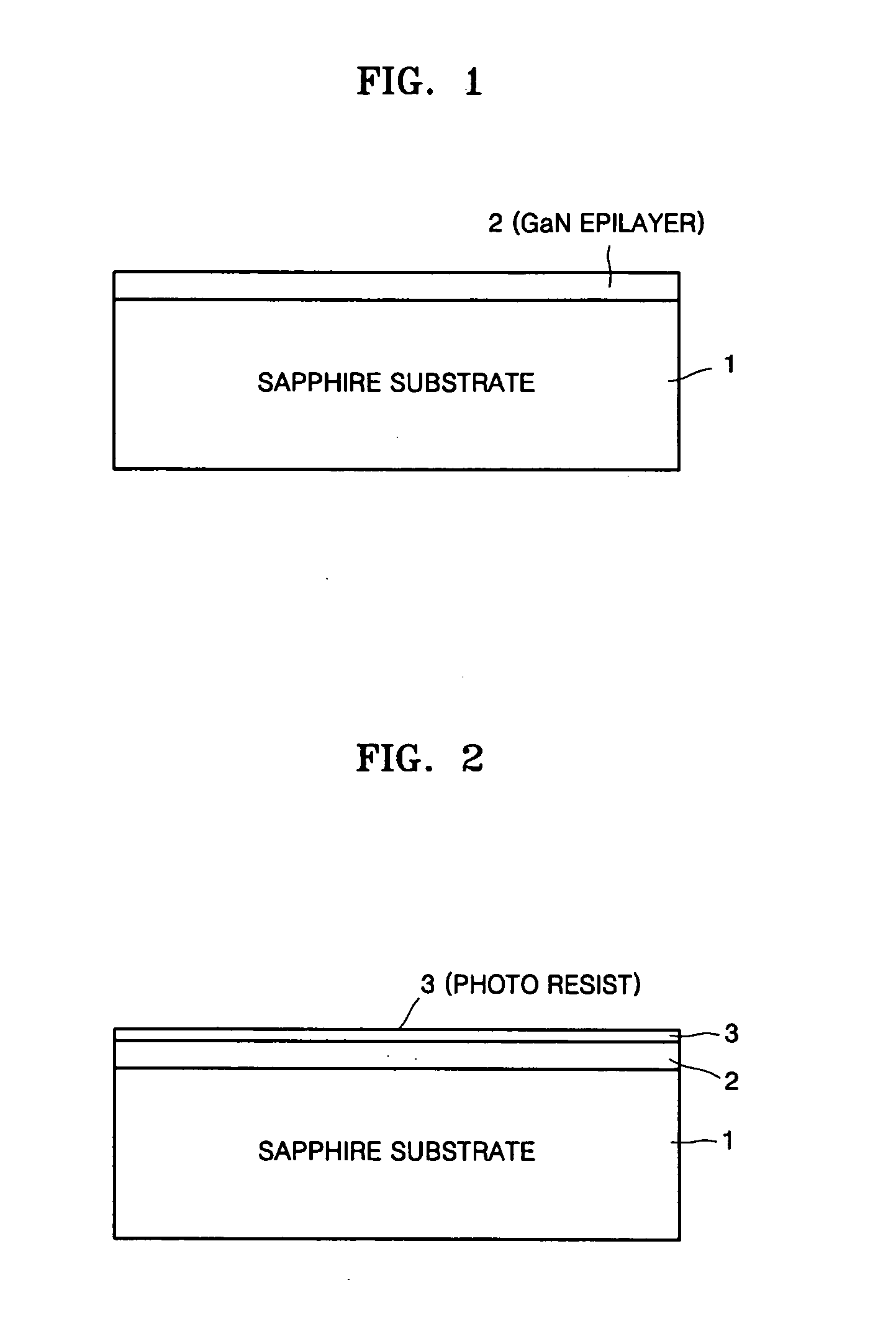
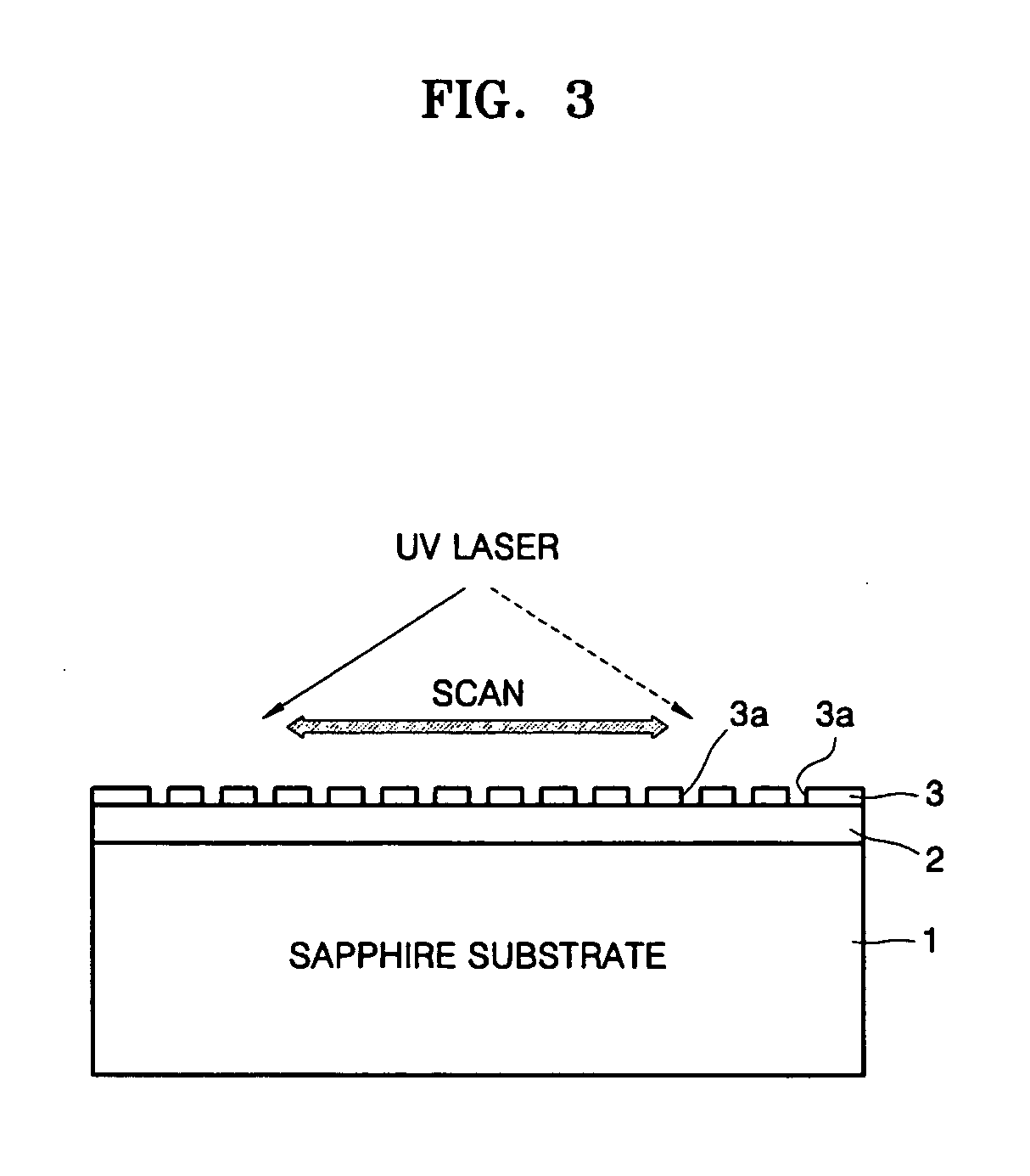
[0016] An epitaxial growth method according to the present invention will now be described more fully hereinafter with reference to the accompanying drawings, in which exemplary embodiments of the invention are shown.

[0017] Referring to FIG. 1, a buffer layer 2 is formed on a prepared single crystalline wafer 1 using a single crystalline semiconductor layer (e.g., a group III nitride semiconductor layer, specifically, a GaN crystalline layer for example). In this case, the single crystalline wafer 1 may be formed of, for example, Si, GaAs, SiC, GaN, or Al2O3 (sapphire). Also, the buffer layer 2 may be formed by stacking a material of the same kind as the material of the wafer 1. For example, the buffer layer 2 may be formed by growing a GaN crystalline layer on a GaN wafer. Alternatively, the buffer layer 2 may be formed by stacking a material of a different kind from the material of the wafer 1. For example, the buffer layer 2 may be formed by growing a GaN crystalline layer on an...


PUM


Abstract

Provided is an epitaxial growth method for forming a high-quality crystalline growth semiconductor wafer. The method includes forming a buffer layer on a single crystalline wafer using a single crystalline material; forming a mask layer on the buffer layer; forming a plurality of holes in the mask layer using a laser to expose portions of the buffer layer; forming wells having a predetermined depth in the exposed portions of the buffer layer by injecting an etchant into the holes; removing the mask layer and annealing the buffer layer to form a porous buffer layer having cavities obtained by the wells; and forming a crystalline material layer on the porous buffer layer using an epitaxial growth process.

Description

CROSS-REFERENCE TO RELATED PATENT APPLICATION [0001] Priority is claimed to Korean Patent Application No. 10-2005-0005024, filed on Jan. 19, 2005, in the Korean Intellectual Property Office, the disclosure of which is incorporated herein in its entirety by reference. BACKGROUND OF THE INVENTION [0002] 1. Field of the Invention [0003] The present invention relates to an epitaxial growth method and more particularly, to a GaN epitaxial growth method. [0004] 2. Description of the Related Art [0005] A substrate on which an epitaxial layer is formed using an epitaxial growth method may be bent and many crystalline defects may arise in the epitaxial layer due to lattice mismatch and a difference in coefficient of thermal expansion between the substrate and the epitaxial layer. Thus, it is necessary to overcome the above-described problems while forming a single crystalline semiconductor material layer using the epitaxial growth method. [0006] U.S. Pat. No. 6,579,359 discloses a technique ...

Claims


Application Information

Patent Timeline
Patent Type & Authority Applications(United States)
IPC IPC(8): H01L21/20
CPCC30B25/04H01L21/0237H01L21/0242H01L21/02458H01L21/02513H01L21/0254H01L21/0262F26B21/02F26B3/04F26B2200/06F26B2200/16
Inventor PARK, SUNG-SOO
Owner SAMSUNG CORNING PRECISION MATERIALS CO LTD
Why Eureka
Try Eureka