
Method for measuring peak carrier concentration in ultra-shallow junctions

a peak carrier and ultra-shallow junction technology, applied in the field of optical devices, can solve the problems of large difficulty in locating near the surface with desired carrier concentration, damage that is typically proportional to the implantation, and damage that is not uniform

Inactive Publication Date: 2006-07-27
THERMA WAVE INC
View PDF12 Cites 14 Cited by
  • Summary
  • Abstract
  • Description
  • Claims
  • Application Information

AI Technical Summary

Benefits of technology

"The patent text describes a system for non-destructive inspection of semiconductor wafers using optical metrology techniques. The system uses a pump laser to create a periodic excitation in the sample, which causes localized periodic excitation. The resulting changes in surface reflectivity of the sample are measured using a probe beam directed at a portion of the sample. The system measures carrier concentration and depth in semiconductor wafers by inducing thermal or plasma waves in the sample and monitoring the resulting changes in reflectivity. The system is also used to measure the damage caused by ion implantation in semiconductor wafers. The technical effects of the patent text are improved non-destructive inspection of semiconductor wafers using optical metrology techniques and improved accuracy in measuring carrier concentration and depth in semiconductor wafers."

Problems solved by technology

The ion implantation damages the crystal lattice as incoming ions come to rest.
This damage is typically proportional to the concentration and depth of ions within the crystal lattice.
However, keeping the USJ profile abrupt and close to the surface with desired carrier concentration is a big challenge.
These techniques are capable of providing detailed USJ profile information, but at the expense of a turnaround time that is usually measured in days or even weeks or at the expense of damaging the surface with contacts.
While USJ depth and abruptness can be characterized using this method in the above cited patent application, no reliable non-contact and non-destructive technique has been described to monitor the peak carrier concentration in USJ samples.

Method used


Image

  • Method for measuring peak carrier concentration in ultra-shallow junctions
  • Method for measuring peak carrier concentration in ultra-shallow junctions
  • Method for measuring peak carrier concentration in ultra-shallow junctions

Examples


Embodiment Construction

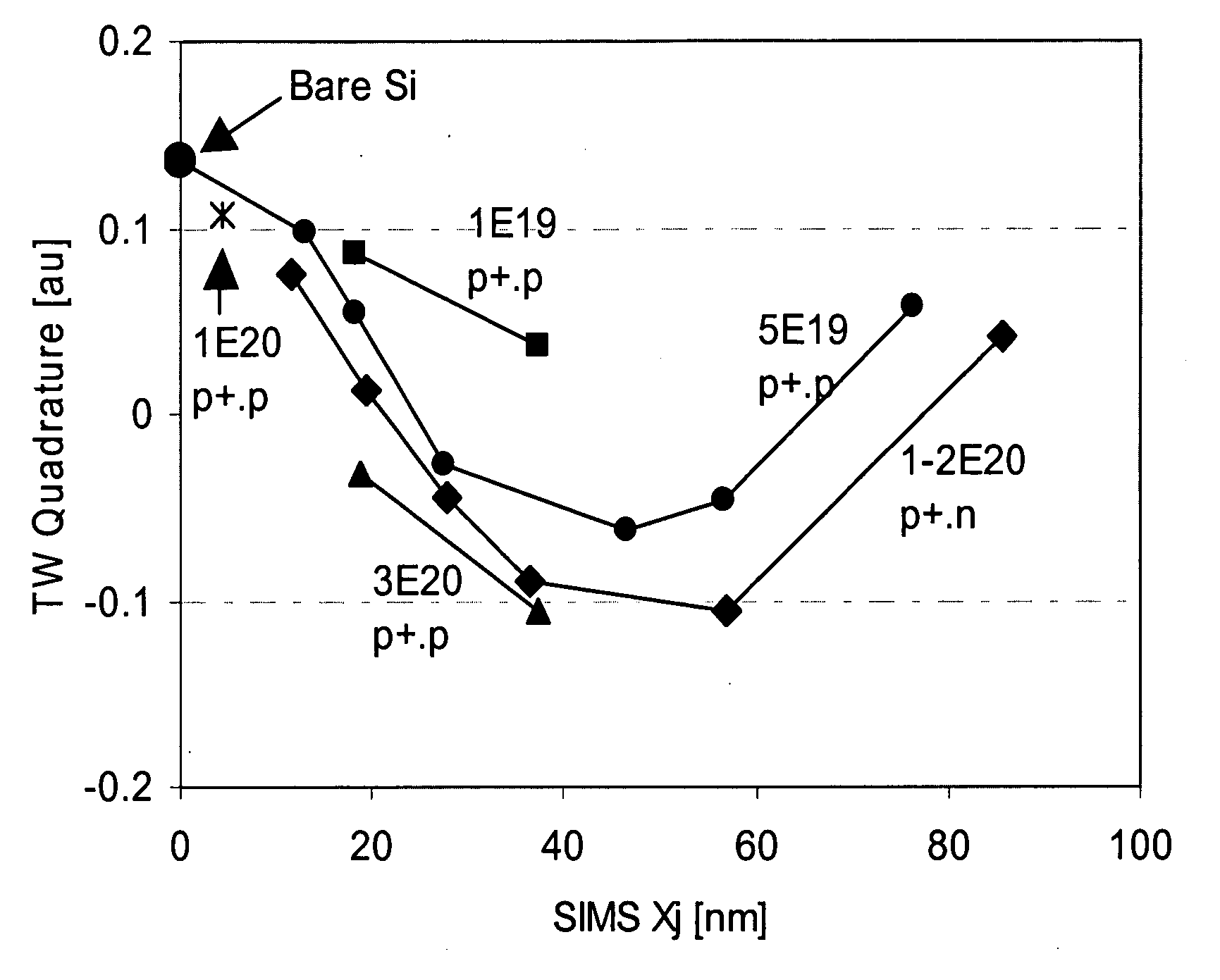
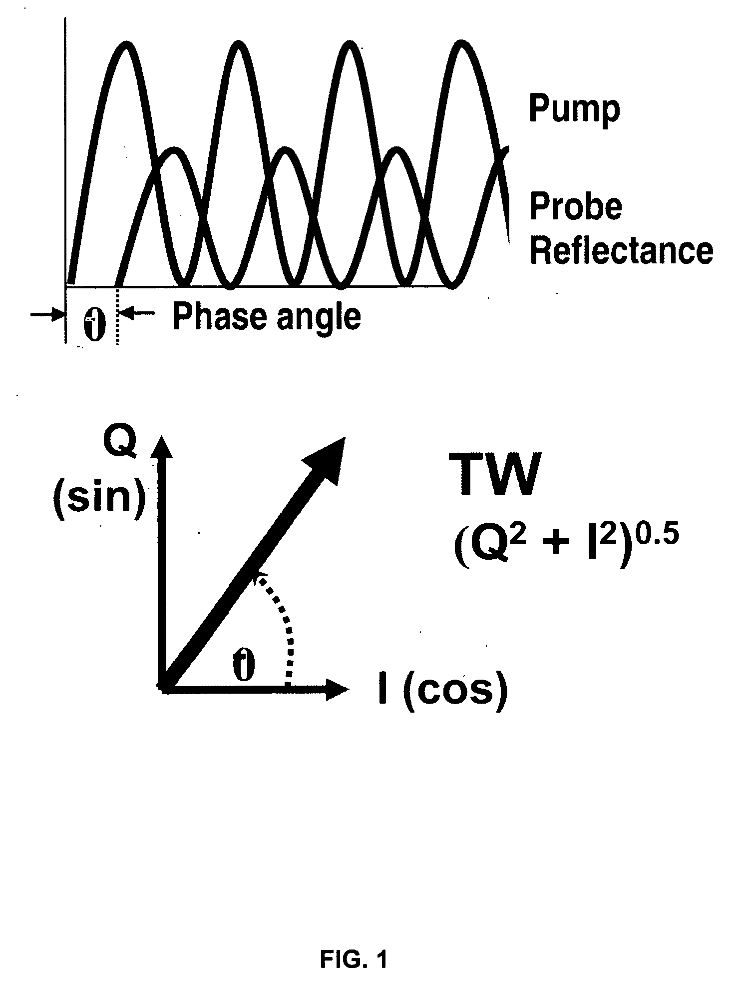
[0028] The present invention provides a method for simultaneously monitoring the carrier concentration C and (if desirable) USJ junction depth Xj in non-destructive and non-contact manner. For this method, a PMR-like optical metrology tool is used on USJ samples in a manner similar to that described in U.S. Patent Publication No. 2005 / 0083528, cited above. In the latter case, I-Q representation of the measurements are used to monitor implant dose, damage and depth. Here we use similar information to derive carrier concentration.

[0029] The behavior of the quadrature component of the TW signal for different USJ junction depths and peak carrier levels is illustrated in FIG. 4. As can be seen in FIG. 4, these data sets display the expected cosine-like junction depth dependence for fixed doparit level, with a zero value at approximately 24 nm junction depth. Further, it can be seen that the cosine correlation curve for the more highly doped data series is shifted downwards. Other data w...


PUM


Abstract

A method is disclosed for determining peak carrier concentration in ultra shallow junctions of semiconductor samples. A region of the surface of the sample is periodically excited. The effects of the excitation are monitored by a probe beam. Synchronous detection produces in-phase (I) and quadrature (Q) signals. These signals are compared to signals obtained from calibration samples to evaluate peak carrier concentration.

Description

PRIORITY [0001] This application claims priority from U.S. Provisional Application Ser. No. 60 / 645,627, filed Jan. 21, 2005.TECHNICAL FIELD [0002] The subject invention relates to optical devices used to non-destructively evaluate semiconductor wafers. In particular, the present invention relates to systems for measuring carrier concentration in semiconductor samples. BACKGROUND OF THE INVENTION [0003] As geometries continue to shrink, manufacturers have increasingly turned to optical techniques to perform non-destructive inspection and analysis of-semiconductor wafers. The basis for these techniques is the notion that a sample may be examined by analyzing the reflected energy that results when an optical beam is directed at a sample. This type of inspection and analysis is known as optical metrology and is performed using a range of different optical techniques. [0004] One widely used type of optical metrology system includes a pump laser. The pump laser is switched on and off to c...

Claims


Application Information

Patent Timeline
Patent Type & Authority Applications(United States)
IPC IPC(8): H01L21/66G01R31/26
CPCG01N21/1717G01N2021/1725G01R31/2648G01R31/2656
Inventor SALNIK, ALEXNICOLAIDES, LENAOPSAL, JONBAKSHI, MIRA
Owner THERMA WAVE INC
Learn More