Vertical carbon nanotube transistor integration

a technology of carbon nanotubes and transistors, applied in the field of vertical carbon nanotube transistor integration, can solve the problems of lagging nfet performance of pfet devices and pfet device performance, and achieve the effect of improving packing density

Active Publication Date: 2006-08-03
GLOBALFOUNDRIES US INC
View PDF16 Cites 58 Cited by
  • Summary
  • Abstract
  • Description
  • Claims
  • Application Information

AI Technical Summary

Benefits of technology

[0007] The present invention overcomes the drawbacks with prior art semiconductor devices including logic gates by integrating a vertical carbon nanotube transistor with a horizontal semiconductor device such as a FET or bipolar transistor in which the carbon nanotube transistor and the horizontal semiconductor device have at least one common, i.e., shared, node. The term “node” is used in the present invention to denote any term

Problems solved by technology

Drawbacks in such technologies include pFET device performance lagging the nFET due to lower mobility and separation requirements between the nFET and the pFET due to

Method used


Image

  • Vertical carbon nanotube transistor integration
  • Vertical carbon nanotube transistor integration
  • Vertical carbon nanotube transistor integration

Examples


Embodiment Construction

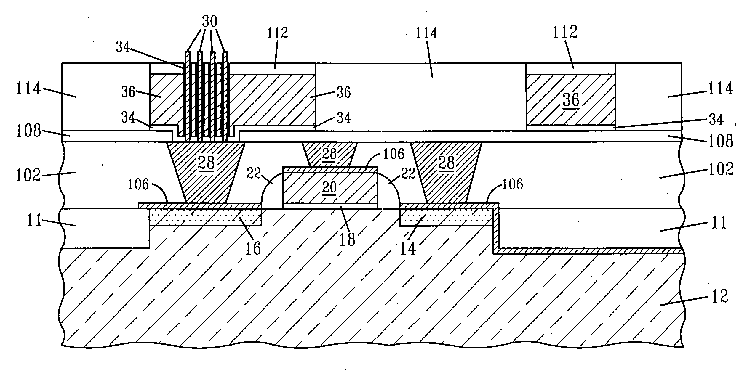
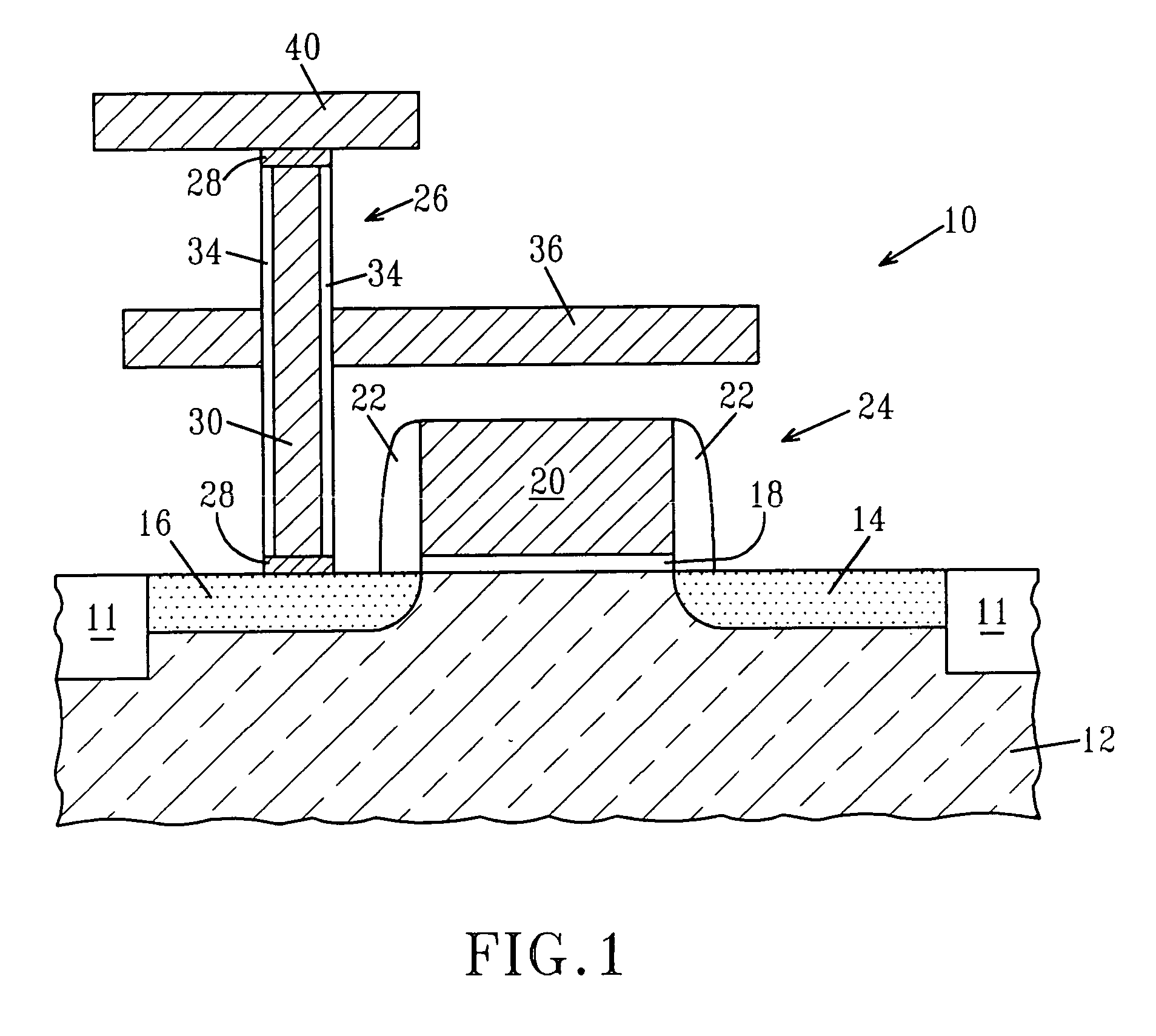
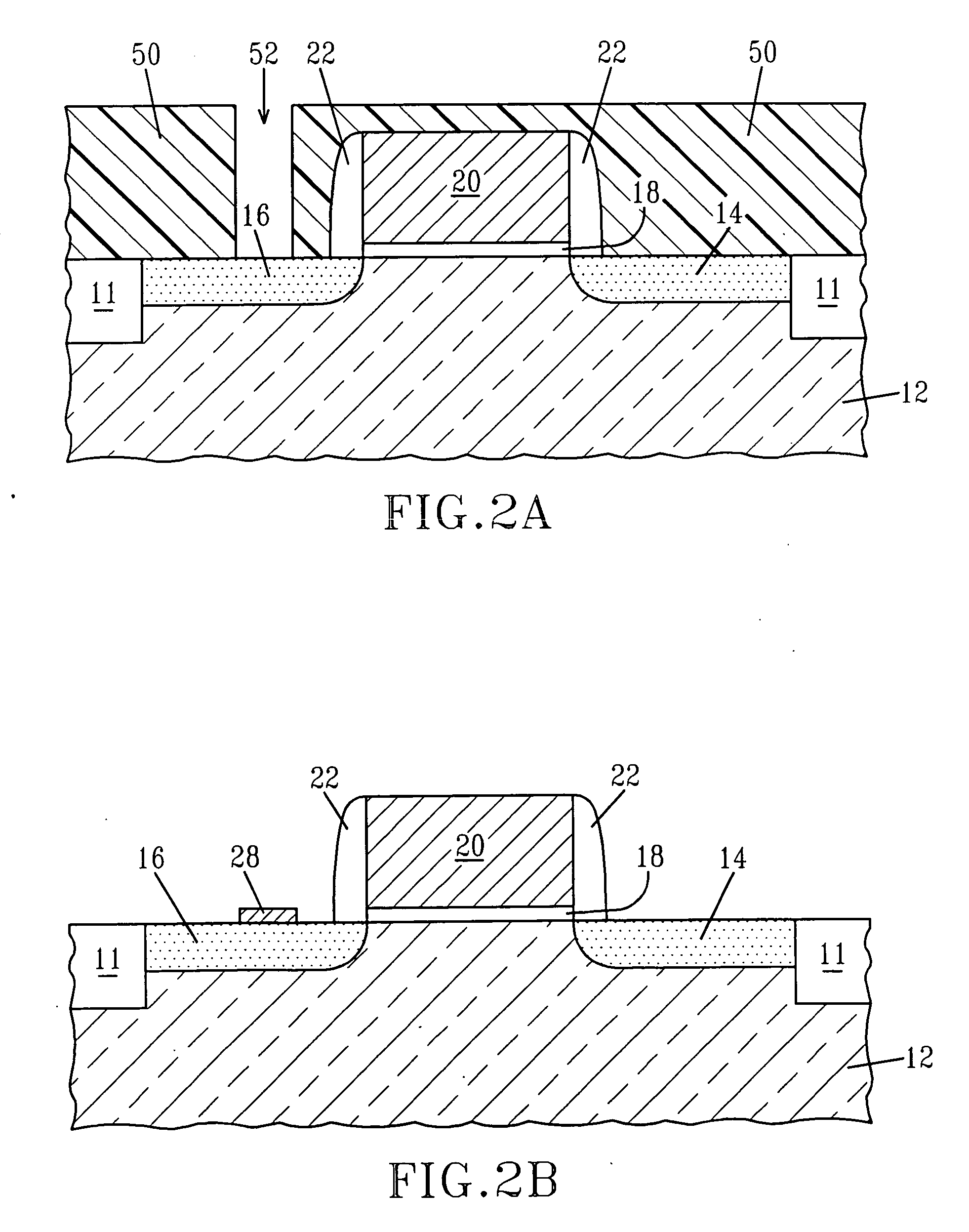
[0017] The present invention, which provides a hybrid semiconductor structure including at least one vertical carbon nanotube transistor and at least one horizontal semiconductor device as well as a method of fabricating the same, will now be described in greater detail by referring to the accompanying drawings.

[0018] It is noted that the drawings of the present invention illustrate one possible embodiment in which the horizontal semiconductor device is a FET. Although such an embodiment is described and illustrated in detail, the present invention also contemplates other embodiments in which other horizontal semiconductor devices such as bipolar transistors, double-gated devices, diodes, capacitors, resistors and the like are used in place of the horizontal FET. The horizontal semiconductor devices can include a combination of devices such as, for example, a combination of a bipolar device and a FET device. In cases in which other horizontal semiconductor devices are used, the bas...


PUM


Abstract

A hybrid semiconductor structure which includes a horizontal semiconductor device and a vertical carbon nanotube transistor, where the vertical carbon nanotube transistor and the horizontal semiconductor device have at least one shared node is provided. The at least one shared node can include, for example, a drain, source or gate electrode of a FET, or an emitter, collector, or base of a bipolar transistor. A method of forming the inventive hybrid semiconductor structure having at least one shared node between the vertical carbon nanotube transistor and the horizontal semiconductor device is also provided.

Description

FIELD OF THE INVENTION [0001] The present invention relates to a semiconductor structure and to a method of fabricating the same. More particularly, the present invention relates to a hybrid semiconductor structure which includes a vertical carbon nanotube transistor and a horizontal semiconductor device where the carbon nanotube transistor and the horizontal semiconductor device have at least one shared node, i.e., terminal, and a method of forming the hybrid semiconductor structure. BACKGROUND OF THE INVENTION [0002] In the field of molecular electronics, few materials show as much promise as carbon nanotubes that comprise hollow cylinders of graphite that have a diameter of a few Angstroms. Nanotubes can be implemented in electronic devices, such as, for example, diodes and transistors, depending on the nanotube characteristics. Nanotubes are unique for their size, shape and physical properties. For example, carbon based nanotubes resemble a hexagonal lattice of carbon rolled int...

Claims


Application Information

Patent Timeline
IPC IPC(8): H01L29/06
CPCB82Y10/00H01L21/823412H01L21/823425H01L21/823487H01L27/0688H01L27/0705H01L27/286H01L51/0048H01L51/057Y10S977/938H10K19/20H10K85/221H10K10/491
Inventor FURUKAWA, TOSHIHARUHAKEY, MARK C.HORAK, DAVID V.KOBURGER, CHARLES W. IIIMASTERS, MARK E.MITCHELL, PETER H.
Owner GLOBALFOUNDRIES US INC
Why Eureka
Try Eureka