Method of fabricating a thin film

a thin film and fabrication method technology, applied in the direction of solid-state devices, coatings, plasma techniques, etc., can solve the problems of insufficient density of thin film, difficult control of thin film growth, and low speed of thin film deposition

Inactive Publication Date: 2006-08-03
SAMSUNG ELECTRONICS CO LTD
View PDF11 Cites 117 Cited by
  • Summary
  • Abstract
  • Description
  • Claims
  • Application Information

AI Technical Summary

Problems solved by technology

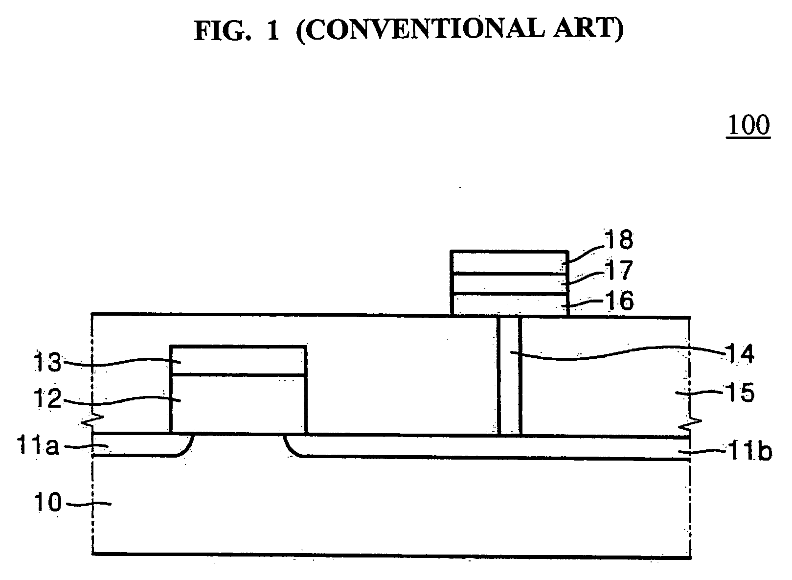
If a thin film is deposited using the PVD process, it may be difficult to control the thin film growth, the speed of deposition of the thin film may be lower, and the thin film may not have a sufficient density.
Additionally, the thin film may be difficult to form in smaller regions.
Heat loss may thereby be increased due to the increased contact area.
Therefore, it may be difficult to employ conventional PRAMs at higher integrations.

Method used


Image

  • Method of fabricating a thin film
  • Method of fabricating a thin film

Examples


Embodiment Construction

[0018] Detailed illustrative example embodiments of the present invention are disclosed herein. However, specific structural and functional details disclosed herein are merely representative for purposes of describing example embodiments of the present invention. Example embodiments of the present invention may, however, be embodied in many alternate forms and should not be construed as limited to the embodiments set forth herein.

[0019] Accordingly, while example embodiments of the invention are susceptible to various modifications and alternative forms, specific embodiments thereof are shown by way of example in the drawings and will herein be described in detail. It should be understood, however, that there is no intent to limit example embodiments of the invention to the particular forms disclosed, but conversely, example embodiments of the invention are to cover all modifications, equivalents, and alternatives falling within the spirit and scope of the invention. Like numbers m...


PUM

PropertyMeasurementUnit
densityaaaaaaaaaa
operating temperatureaaaaaaaaaa
resistanceaaaaaaaaaa

Abstract

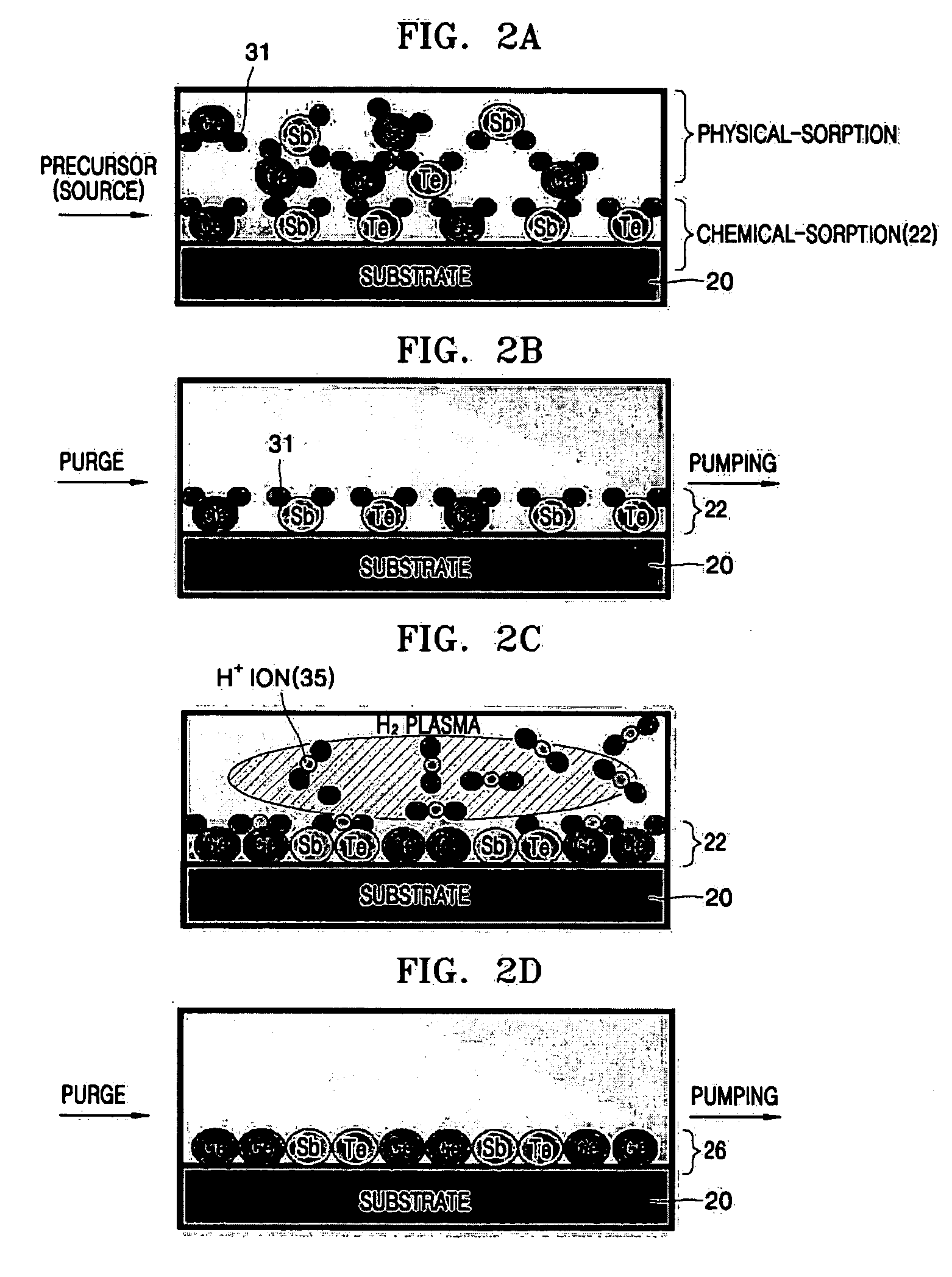
Methods of fabricating a thin film. An example method includes forming a GeSbTe thin film on a surface of a substrate by chemically reacting a first precursor including germanium (Ge), a second precursor including antimony (Sb), and a third precursor including tellurium (Te) in a reaction chamber and processing the surface of the GeSbTe thin film with hydrogen plasma. Another example method includes injecting at least one precursor into a reactor chamber and depositing the at least one precursor onto a substrate within the reactor chamber using a chemical vapor deposition process so as to form the thin film.

Description

PRIORITY STATEMENT [0001] This application claims priority of Korean Patent Application No. 10-2005-0008753, filed on Jan. 31, 2005, in the Korean Intellectual Property Office, the disclosure of which is incorporated herein in its entirety by reference. BACKGROUND OF THE INVENTION [0002] 1. Field of the Invention [0003] Example embodiments of the present invention relate to a method of fabricating a thin film, and more particularly to a method of fabricating a thin film having reduced impurities. [0004] 2. Description of the Related Art [0005] A phase-change material may be selectively converted between crystalline and amorphous states based on an operating temperature. A phase-change material may have a lower resistance when in a crystalline state as compared to the phase-change material in an amorphous state. In the crystalline state, the phase-change material may be characterized as having a systematic or ordered arrangement of atoms. The phase-change material may be reversibly c...

Claims


Application Information

Patent Timeline
Patent Type & Authority Applications(United States)
IPC IPC(8): C23C16/00
CPCC23C16/305C23C16/56H01L45/06H01L45/1233H01L45/144H01L45/1616H01L27/2436H10B63/30H10N70/231H10N70/826H10N70/8828H10N70/023H01L21/02205H01L21/02274
Inventor LEE, JUNG-HYUNLEE, CHARIG-SOOKHANG, YOON-HO
Owner SAMSUNG ELECTRONICS CO LTD
Why Eureka
Try Eureka