Device packages

a technology of device package and integrated circuit, which is applied in the direction of semiconductor/solid-state device details, manufacturing tools, non-electric welding apparatus, etc., can solve the problems of unreliable bonding of wires with dies, capacitors,/or lead frames, and substantially compromised assembly process, so as to avoid unsatisfactory interaction between tools and package geometry

Active Publication Date: 2006-08-03
BELL SEMICON LLC
View PDF3 Cites 15 Cited by
  • Summary
  • Abstract
  • Description
  • Claims
  • Application Information

AI Technical Summary

Benefits of technology

[0011] Surprisingly it has been found that the assembly process has been substantially compromised for devices including wire electrical interconnection loops with geometries having 1) a loop height to wire length aspect ratio greater than 2:1 for 2) a loop height greater than 10 mils. (Such geometry satisfying these two criteria are denominated high aspect ratio geometries in the context of this invention. The wire length is the distance along the wire between bonding points forming the electrical connection between the die and another component. The loop height is the distance measured normal to the major surface of the heat sink to the point on the wire furthest above this surface.) The angle limitations induced by th...

Problems solved by technology

Surprisingly it has been found that the assembly process has been substantially compromised for devices including wire electrical interconnection loops with geometries having 1) a loop height to wire length aspect ratio greater...

Method used


Image

  • Device packages
  • Device packages
  • Device packages

Examples


Embodiment Construction

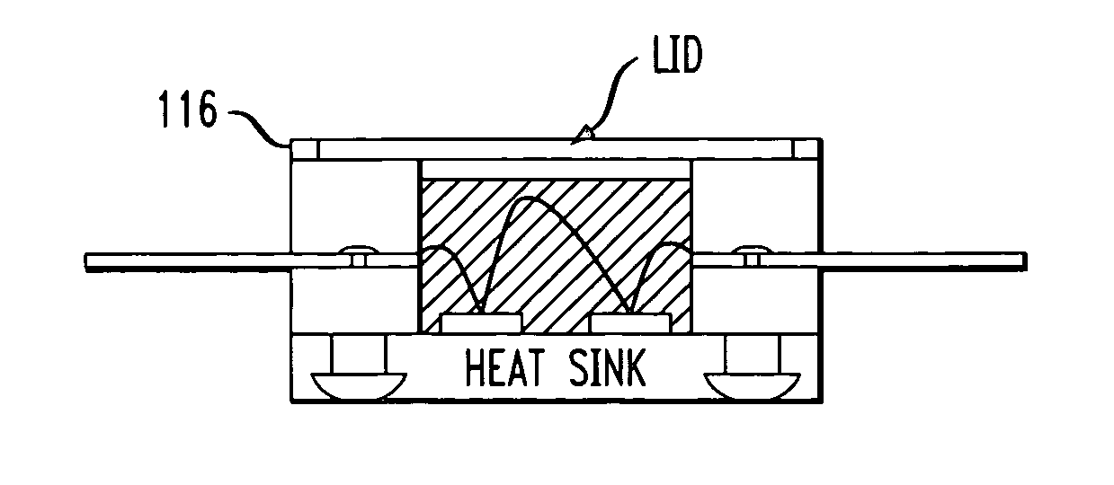
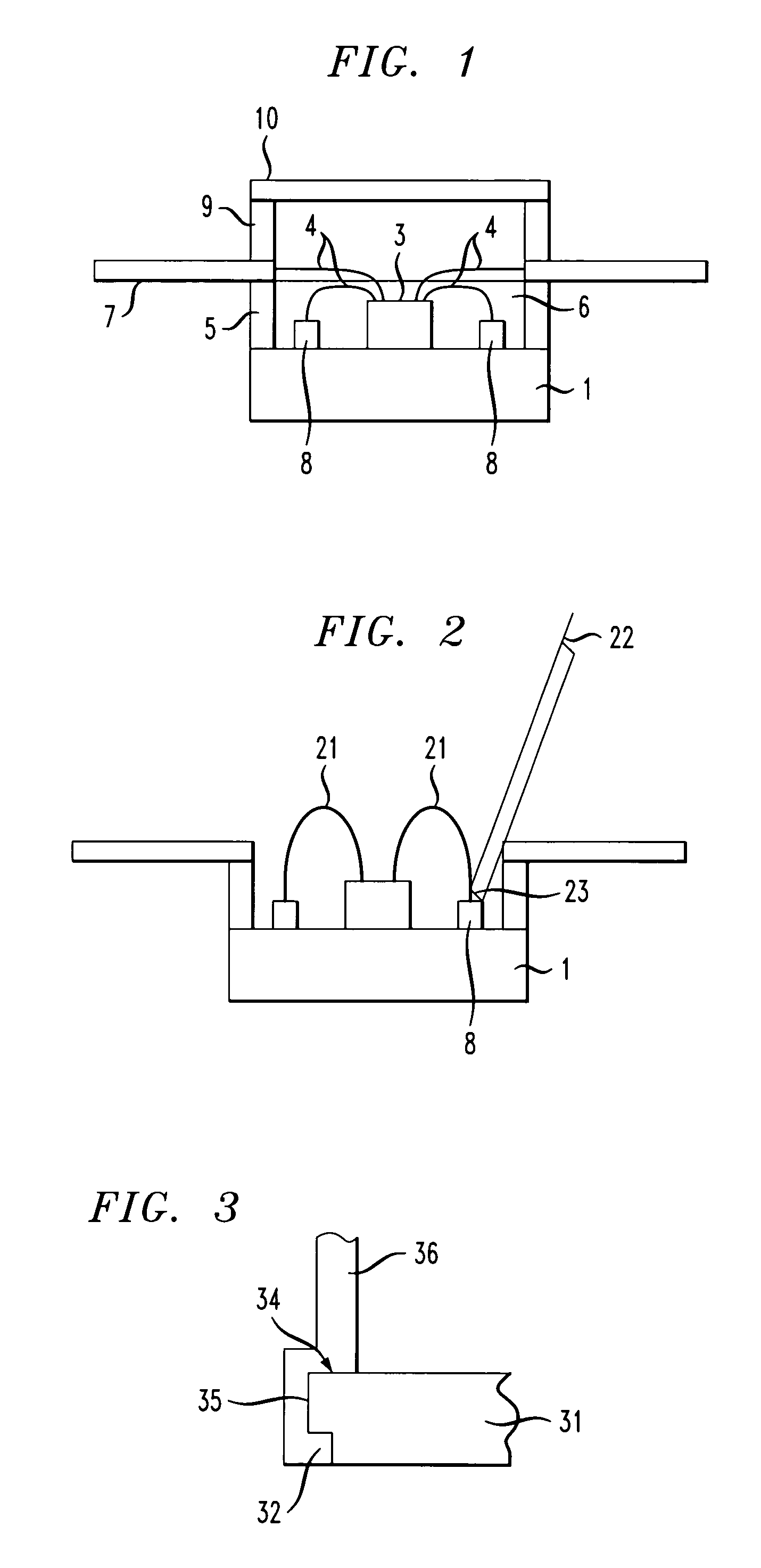
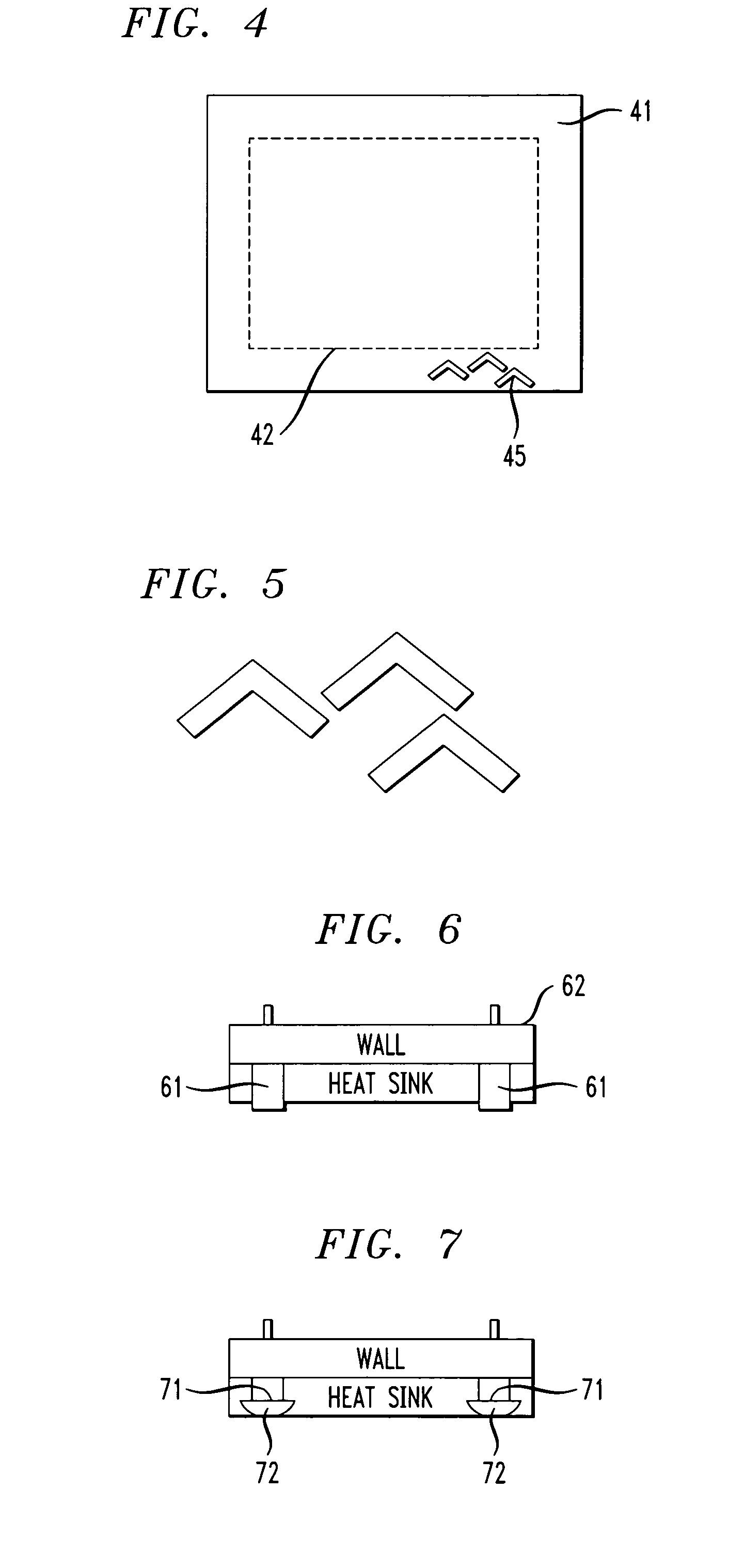
[0015] Surprising results have been found for devices with 1) at least one lead wire having loop height to wire length aspect ratio greater than 2:1, especially greater than 5:1, and 2) a loop height greater than 10 mils, (i.e. a high aspect geometry in the context of this invention). In particular, the connection between such wire and the lead frame or other point of attachment such as capacitors external to the die are not expeditiously made and tend to suffer inadequate bonding. A number of techniques are possible for avoiding the difficulties induced in the wire bonding process. Generally, wire bonds for wires having high aspect ratio geometries should be made before forming on the heat sink walls with a height greater than the loop height used in the final device configuration. Generally, the maximum loop height varies from 10 mil to 60 mil. (The height of a wall is measured in a direction normal from the major surface of the heat sink it adjoins and the height is given by the ...


PUM

PropertyMeasurementUnit
Angleaaaaaaaaaa
Heightaaaaaaaaaa
Heightaaaaaaaaaa

Abstract

Devices such as amplifiers are built on a heat sink having a perimeter wall surrounding active electronic devices. Surprisingly formation of wire bonds to such devices tends to be degraded if they have an aspect ratio greater than 2:1. This problem is overcome by forming wire bonds before such walls have a height of 30 mils and after bond formation extending the walls to their final height.

Description

CROSS REFERENCE [0001] The subject matter of this application is related to that of U.S. patent application Ser. No.______(Brennan 8-87-11-54-10-6) filed contemporaneously and assigned to a common assignee which is hereby incorporated by reference in its entirety.TECHNICAL FIELD [0002] This invention relates to integrated circuits and in particular to integrated circuits with high aspect ratio wire bonds. BACKGROUND OF THE INVENTION [0003] Many integrated circuits, such as RF amplifiers, generate a substantial amount of heat during operation. For example, contemporary RF amplifiers used in wireless communication systems often operate at temperatures approaching 200 degrees C. Clearly at such elevated temperatures, an efficient approach to dissipating the generated heat is required. Thus the packaging for these integrated circuits is generally formed on a heat sink made of a material e.g. copper containing or aluminum containing composition that has excellent heat conducting properti...

Claims


Application Information

Patent Timeline
IPC IPC(8): H01L21/60
CPCB23K20/005H01L21/52H01L23/10H01L23/24H01L23/36H01L23/49861H01L24/48H01L24/49H01L24/83H01L24/85H01L2224/05599H01L2224/4809H01L2224/48091H01L2224/48137H01L2224/484H01L2224/49109H01L2224/78313H01L2224/83801H01L2224/85181H01L2224/85399H01L2924/01013H01L2924/01027H01L2924/01029H01L2924/01074H01L2924/01082H01L2924/01322H01L2924/14H01L2924/19041H01L2924/00014H01L2924/01006H01L2924/01033H01L2224/78H01L2224/45099H01L2224/85205H01L2224/85207H01L2924/181H01L2224/48139H01L2924/00
Inventor BRENNAN, JOHN M.FREUND, JOSEPH MICHEALGILBERT, JEFFREY JOHNOSENBACH, JOHN WILLIAMSAFAR, HUGO FERNANDO
Owner BELL SEMICON LLC
Why Eureka
Try Eureka