Display device and driving method thereof

a technology of a display device and a driving method, which is applied in the direction of dynamo-electric machines, instruments, supports/enclosements/casings, etc., can solve the problems of lowering the uniformity of image display, deteriorating the tfts, and incompatible a-si tfts with the large display devi

Active Publication Date: 2006-08-10
SAMSUNG DISPLAY CO LTD
View PDF11 Cites 35 Cited by
  • Summary
  • Abstract
  • Description
  • Claims
  • Application Information

AI Technical Summary

Problems solved by technology

However, the a-Si TFTs may be incompatible with the large display devices because of the relatively low field effect mobility of the a-Si TFTs.
In addition, when the a-Si TFTs supply current to the organic light-emitting elements continuously, a transition of threshold voltages is generated which deteriorates the TFTs.
However, damage during the crystallization process using laser annealing technology may cause deviations of the threshold voltages between driving transistors for supplying current to the organic light emitting elements, thereby lowering uniformity of image display.
The pixel circuits that have been proposed to realize the uniform image display over the entire screen by compensating for the deviation between the threshold voltages cannot satisfy the increasing demands for high-density OLEDs, since they have too many TFTs, storage capacitors, and interconnect wiring.

Method used


Image

  • Display device and driving method thereof
  • Display device and driving method thereof
  • Display device and driving method thereof

Examples


Embodiment Construction

[0038] Hereinafter, exemplary embodiments of the present invention will be described in detail with reference to the accompanying drawings.

[0039] In the drawings, the size and relative sizes of the layers, films, and regions may be exaggerated for clarity. Like reference numerals refer to like elements throughout the description of the figures. When an element such as a layer, film, region, or substrate is referred to as being “on” another element, it can be directly on the other element or intervening elements may also be present.

[0040] Hereinafter, an organic light emitting device according to a preferred embodiment of the present invention will be described with reference to FIG. 1 through FIG. 6.

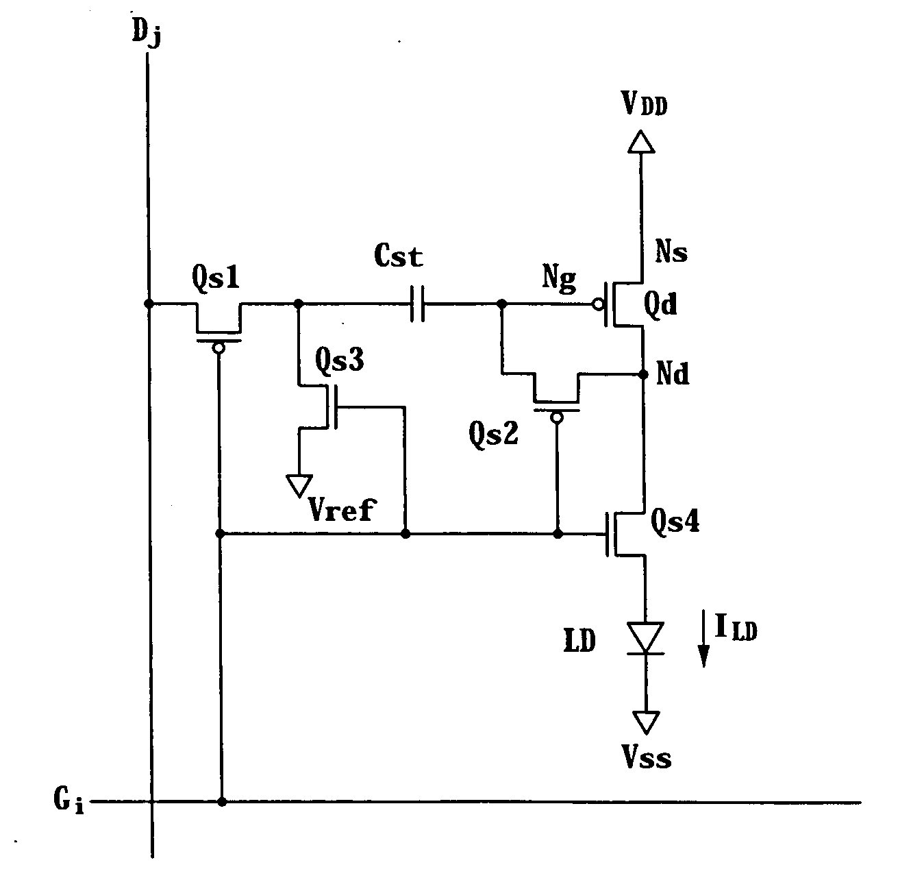
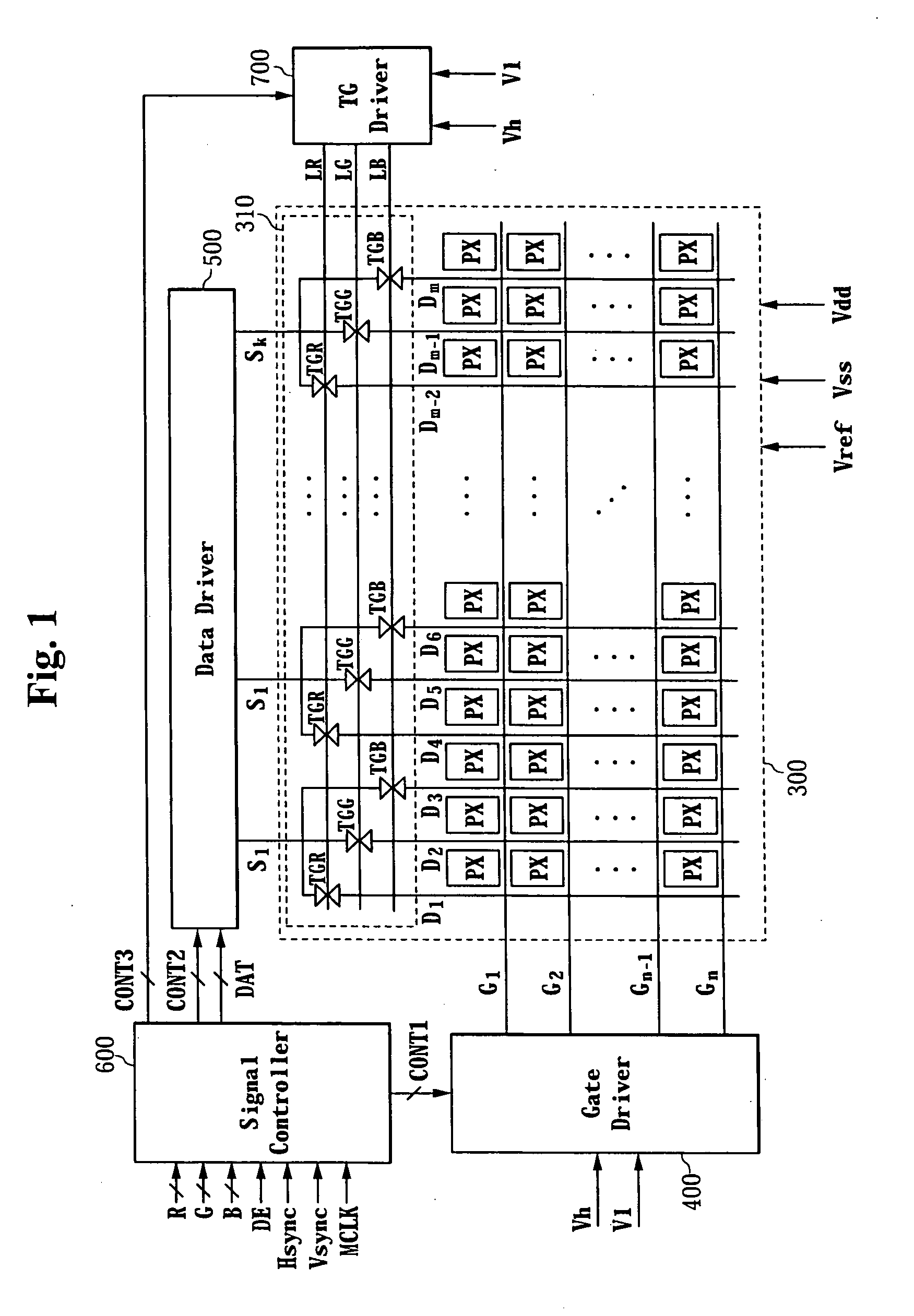
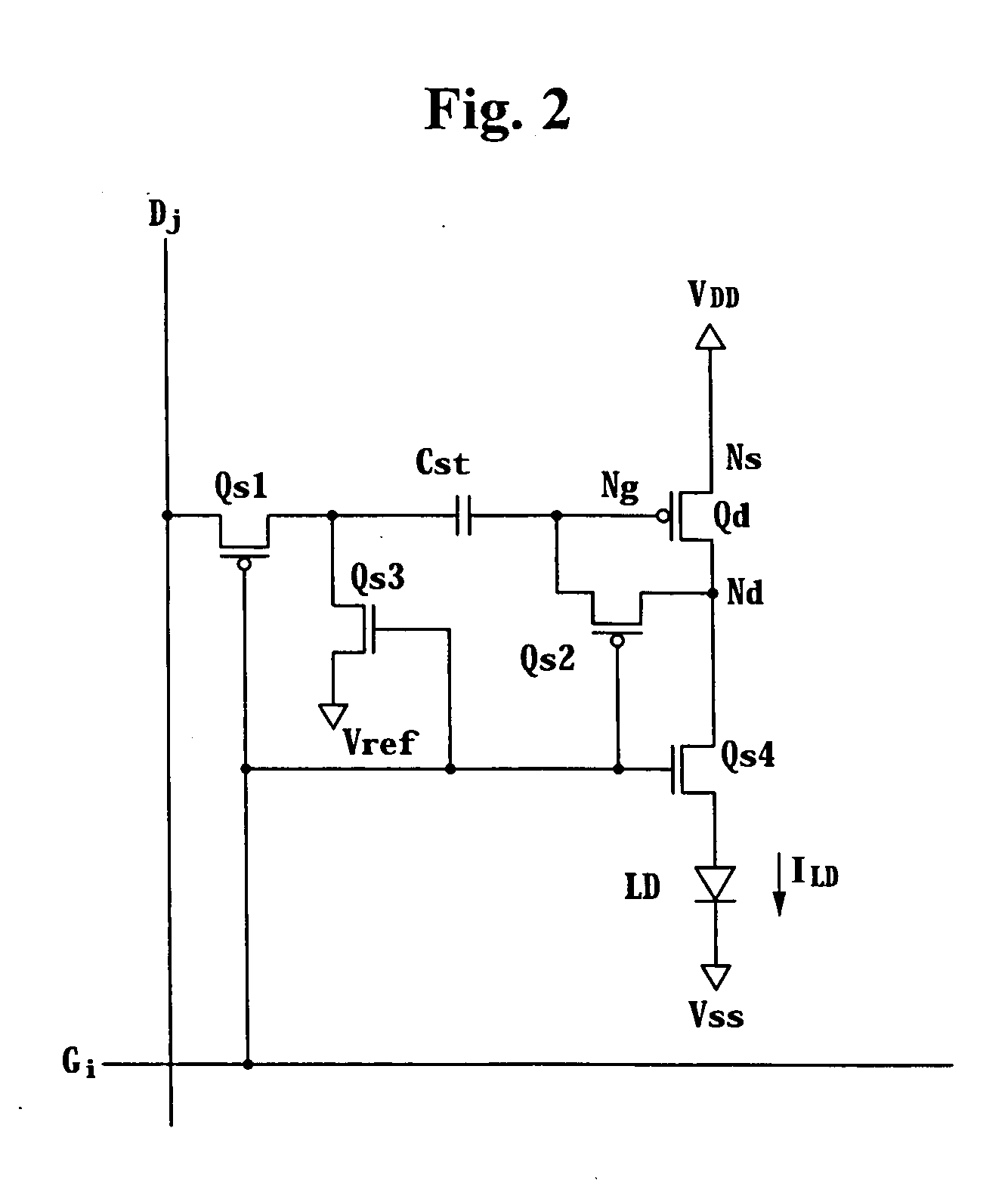
[0041]FIG. 1 is a block diagram of an organic light emitting device according to an exemplary embodiment of the present invention. FIG. 2 is a circuit diagram of a pixel of an organic light emitting device according to an embodiment of the present invention. FIG. 3 is a cross-sectiona...


PUM


Abstract

A display device includes a plurality of data lines, a transmission gate element connected to the data lines, wherein the transmission gate supplies precharge voltages and data voltages to the data lines in response to transmission gate signals, and a plurality of pixels connected to the data lines. Each of the pixels includes: a light emitting element; a capacitor; a driving transistor having a control terminal connected to the capacitor, an input terminal, and an output terminal, wherein the driving transistor supplies a driving current to the light emitting element; a first switch, wherein the first switch diode-connects the driving transistor in response to a gate signal and connects one of the data lines to the capacitor; and a second switch, wherein the second switch supplies a reference voltage to the capacitor in response to the gate signal and connects the driving transistor to the light emitting element, wherein the precharge voltage, the data voltage, and the reference voltage are applied to the capacitor, and wherein the capacitor stores a charging voltage based on the applied data voltage and a threshold voltage of the driving transistor.

Description

CROSS-REFERENCE TO RELATED PATENT APPLICATION [0001] This application claims priority to Korean Patent Application No. 10-2005-0011224, filed on Feb. 7, 2005, in the Korean Intellectual Property Office, the disclosure of which is herein incorporated by reference in its entirety. BACKGROUND OF THE INVENTION [0002] 1. Technical Field [0003] The present invention relates generally to a display device and a method of driving the same. [0004] 2. Description of the Related Art [0005] Organic light emitting devices (OLEDs) utilize fluorescent organic materials that emit light when excited by an electric current. These devices are an increasingly popular form of flat panel display technology due to their self-emitting properties, low power requirements, wide viewing angle, excellent responsiveness, and compatibility with full-motion video. An active matrix organic light-emitting device having a plurality of pixels arranged in matrix form realizes image display by controlling the luminance o...

Claims


Application Information

Patent Timeline
Patent Type & Authority Applications(United States)
IPC IPC(8): G09G3/30
CPCG09G3/3233G09G2300/0819G09G2300/0842G09G2300/0866G09G2320/043H02K7/083H02K7/116H02K7/1807H02K9/02H02K2205/09
Inventor PARK, KEE-CHANKIM, II-GONMAENG, HO-SUK
Owner SAMSUNG DISPLAY CO LTD
Why Eureka
Try Eureka