Phase change memory device

a phase change memory and semiconductor technology, applied in static storage, digital storage, instruments, etc., can solve the problems of high integration and other problems, and achieve the effects of high integration, reduced layout area per bit, and sufficient rewriting curren

Active Publication Date: 2006-08-10
MICRON TECH INC
View PDF19 Cites 28 Cited by
  • Summary
  • Abstract
  • Description
  • Claims
  • Application Information

AI Technical Summary

Benefits of technology

[0017] As described above, according to the present invention, a phase change layer is formed on a semiconductor substrate and current can be supplied to a unit configuration including one MOS transistor and a plurality of phase change memory elements via a lower electrode structure. Therefore, since the layout area per bit can be reduced when the gate width of the MOS transistor is increased in order to supply sufficient rewriting current for rewriting data to the plurality of phase change memory elements, it is possible to realize high integration of the phase change memory device.

Problems solved by technology

In this case, the entire chip area increases as the storage capacity increases in the phase change memory, resulting in an obstacle to high integration.

Method used


Image

  • Phase change memory device
  • Phase change memory device
  • Phase change memory device

Examples


Embodiment Construction

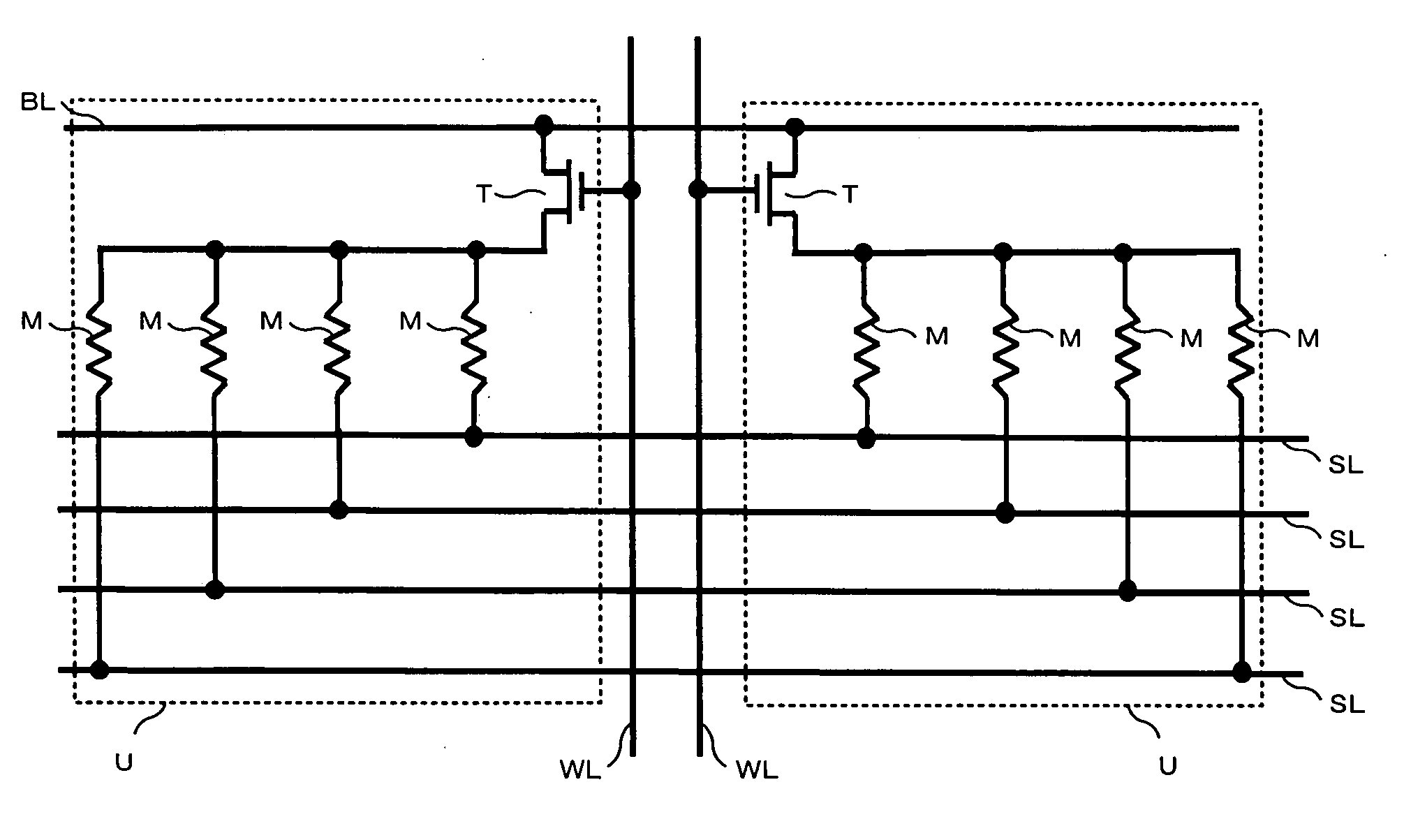
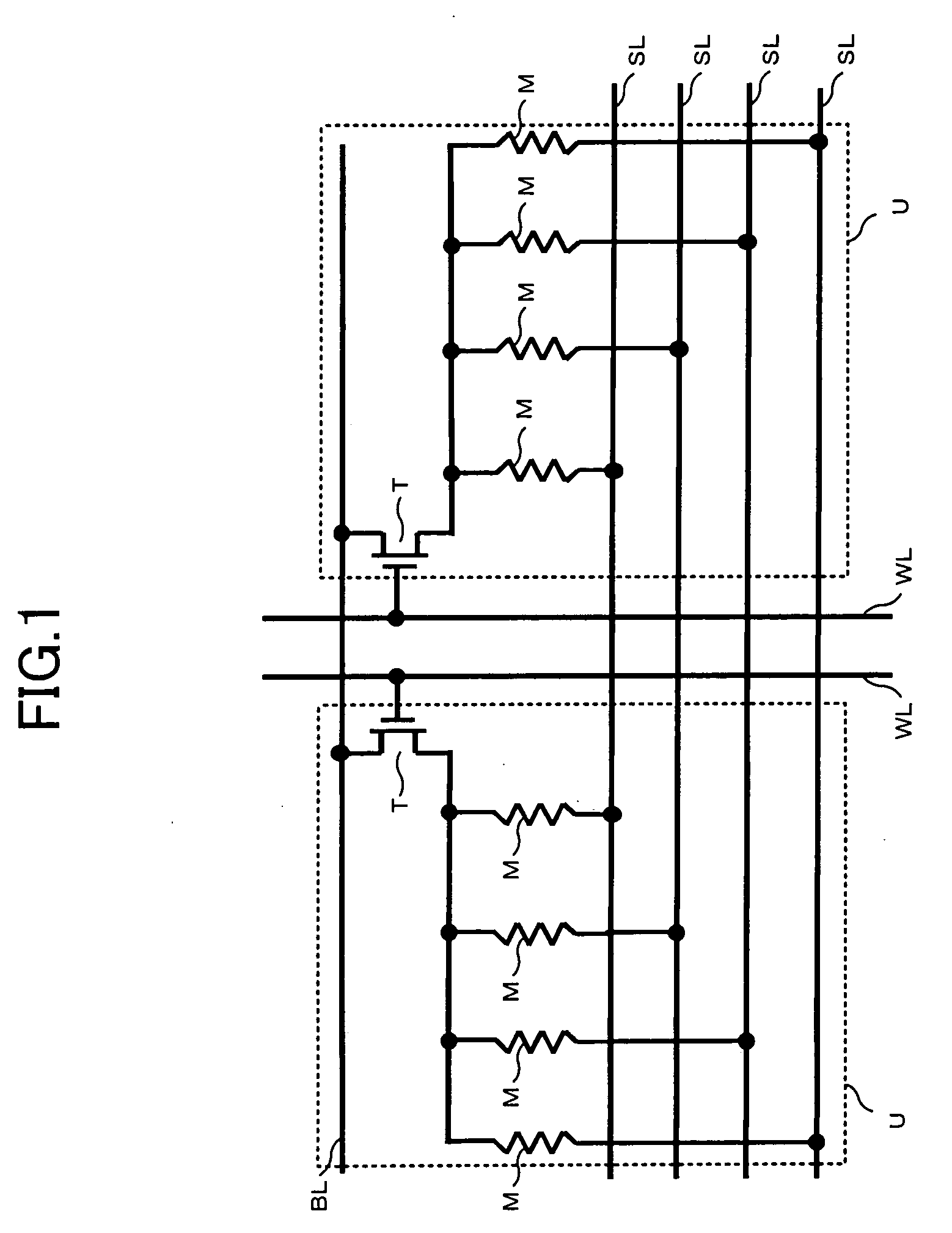
[0041] An embodiment of the invention will be specifically described below with reference to accompanying drawings. This embodiment describes a case in which the invention is applied to a phase change memory device which is a non-volatile semiconductor storage device using the phase change material.

[0042] Referring to FIG. 1, a basic circuit configuration which is a unit configuration of the phase change memory device of this embodiment will be described. In the circuit as shown in FIG. 1, one unit circuit U is composed of a MOS transistor T and four phase change memory elements M commonly connected to the transistor. The four phase change memory elements M are connected to respective different element selection lines SL and supplied with current separately. The entire circuit of the phase change memory device is configured by regularly arranging a large number of unit circuits U having the same configuration. FIG. 1 shows a circuit part including two unit circuits U of the entire ...


PUM

PropertyMeasurementUnit
depthaaaaaaaaaa
thicknessaaaaaaaaaa
thicknessaaaaaaaaaa

Abstract

A phase change memory device, comprising a phase change memory device; a semiconductor substrate; a MOS transistor disposed at each intersection of a plurality of word lines and a plurality of bit lines arranged in a matrix form; a plurality of phase change memory elements for storing data of a plurality of bits, each formed on an upper area opposite to a diffusion layer of the MOS transistor in a phase change layer made of phase change material; a lower electrode structure for electrically connecting each of the plurality of phase change memory elements to the diffusion layer of the MOS transistor.

Description

BACKGROUND OF THE INVENTION [0001] 1. Field of the Invention [0002] The present invention relates to a non-volatile semiconductor device which is constructed on a semiconductor substrate using phase change material and is capable of storing desired data. [0003] 2. Related Art [0004] In recent years, non-volatile memory has been widely used to store data of portable device and the like. As next-generation non-volatile memory, attention is directed toward phase change memory using structural changes of phase change material. For example, the phase change memory has a structure in which a phase change layer is deposited on a semiconductor substrate using a chalcogenide based phase change material, and current is supplied to a predetermined region of the layer via an electrode. Such a structure causes the predetermined region of the phase change layer to change freely between its high-resistance amorphous state and low-resistance crystalline state, and using changes in resistance of the...

Claims


Application Information

Patent Timeline
Patent Type & Authority Applications(United States)
IPC IPC(8): G11C17/06
CPCG11C13/0004G11C13/003G11C2213/78G11C2213/79H10B63/84H10B63/30H10B63/80H10N70/231H10N70/826H10N70/8828
Inventor ASANO, ISAMUFUJI, YUKIONAKAI, KIYOSHIKAWAGOE, TSUYOSHI
Owner MICRON TECH INC
Why Eureka
Try Eureka