Method of manufacturing optical interferance color display

a color display and optical interference technology, applied in the direction of electrical appliances, semiconductor devices, instruments, etc., can solve the problems of poor utilization of light sources, time is not fast, and the sacrificial layers are damaged, so as to improve the optical performance of the optical interference color display, prevent the sacrificial layers from being damaged, and improve the air gap

Inactive Publication Date: 2006-08-10
SNAPTRACK
View PDF99 Cites 26 Cited by
  • Summary
  • Abstract
  • Description
  • Claims
  • Application Information

AI Technical Summary

Benefits of technology

[0014] Accordingly, the present invention is directed to a method of fabricating an optical interference color display. In this method, the thicknesses of the sacrificial layers can be precisely controlled so that better air gaps can be obtained.
[0015] The present invention is also directed to a method of fabricating an optical interference color display. In this method, better air gaps can be formed, and the optical performance of the optical interference color display can be enhanced.
[0042] In the method of fabricating the optical interference color display, materials with different etching rates are used to form sacrificial layers. As a result, the sacrificial layers have different etching rates. While being etched, damage to the sacrificial layers can be prevented, and the better air gaps can be obtained. Accordingly, the optical performance of the optical interference color display can be improved.

Problems solved by technology

However, LCD displays still have some disadvantages.
For example, the angles are not wide enough, the response time is not fast, and requirement of using polarizer results in poor utilization of light source.
That causes impact to the subsequent processes.
Under the described unstable manufacturing processes, yields are declined and manufacturing costs are also increased.

Method used


Image

  • Method of manufacturing optical interferance color display
  • Method of manufacturing optical interferance color display
  • Method of manufacturing optical interferance color display

Examples


first embodiment

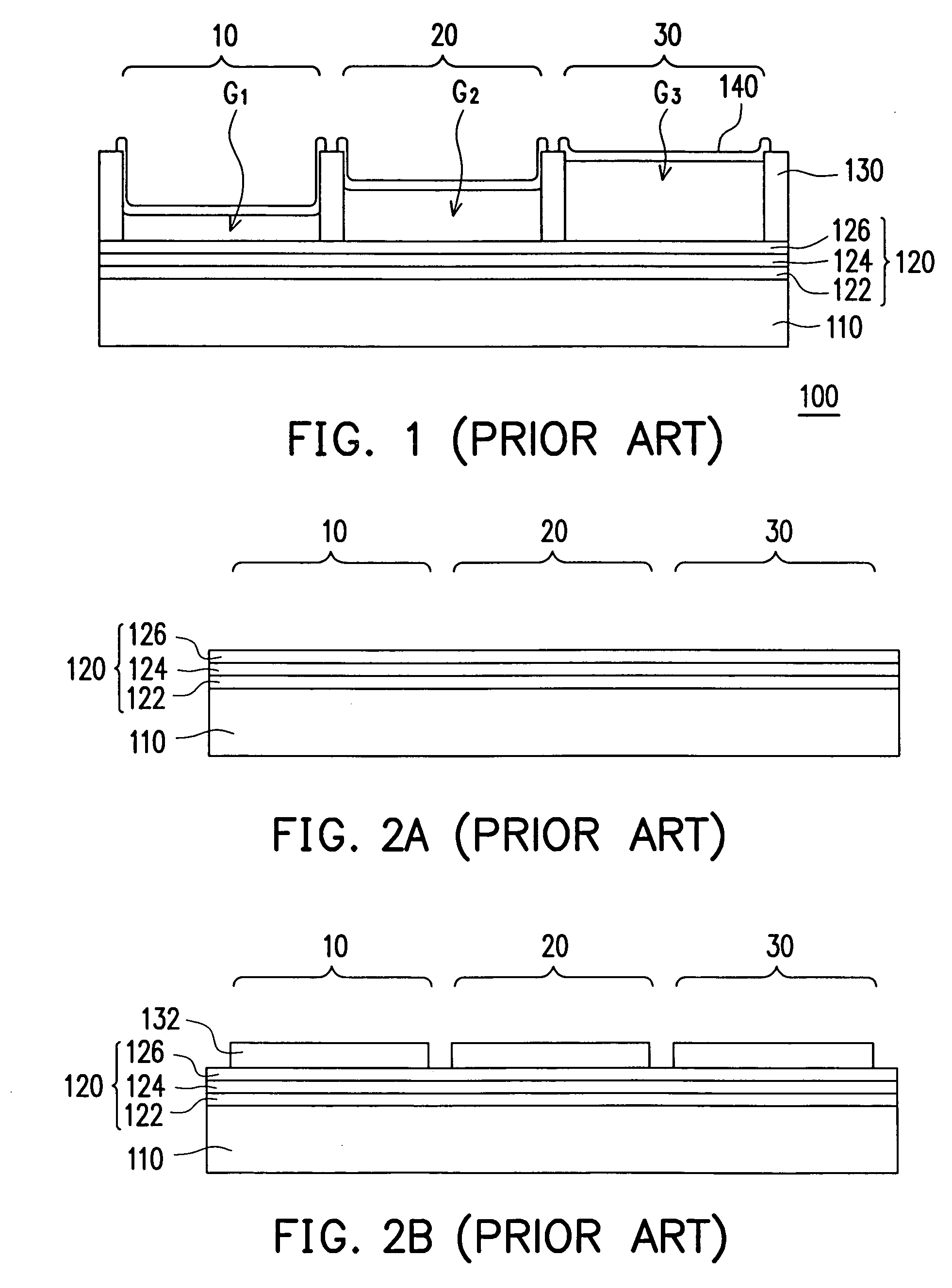
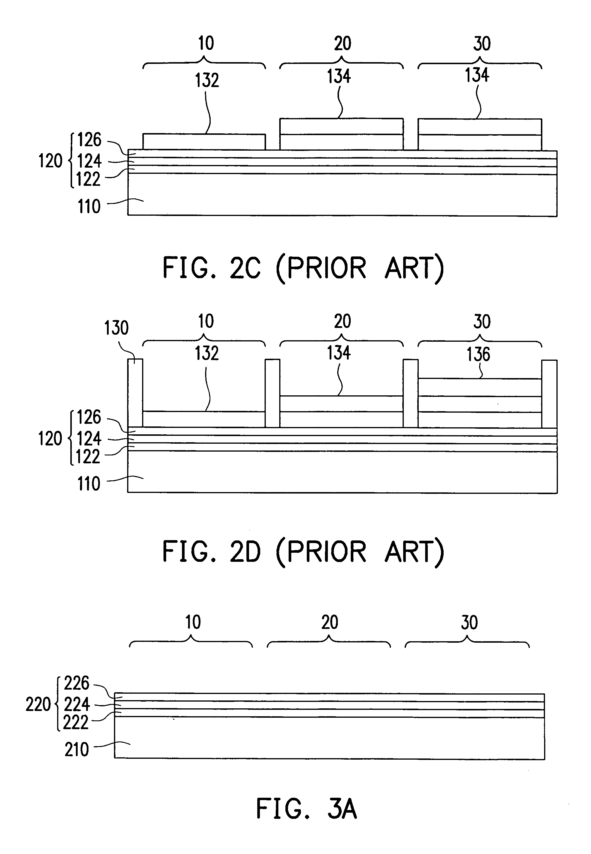
[0048]FIGS. 3A-3F are cross sectional views showing progress of a method of fabricating an optical interference color display according to the first embodiment of the present invention. Referring to FIG. 3A, a transparent substrate 210 is provided. Its material can be, for example, glass or plastic. A first electrode structure 220 is then formed over the transparent substrate 210.

[0049] The method of forming the first electrode structure 220 can be, for example, a physical vapor deposition (PVD) process or other suitable processes, to deposit indium tin oxide (ITO) over the transparent substrate 210. The ITO layer is then patterned by a photolithographic process and an etching process to form a plurality of first transparent electrodes 222. An absorption layer 224 is then deposited over the first electrodes 222 and partial area of the substrate 210 where no first electrodes 222 are formed. In one embodiment of the present invention, the material of the absorption layer 224 can be, ...

second embodiment

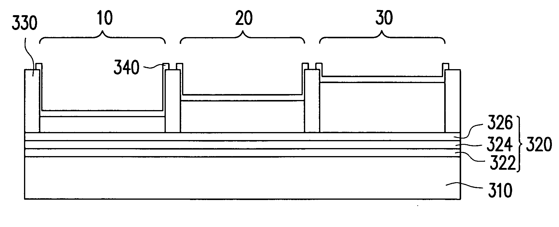
[0060]FIGS. 4A-4F are cross sectional views showing progress of a method of fabricating an optical interference color display according to the second embodiment of the present invention. Referring to FIG. 4A, the steps are similar to those shown in FIG. 3A. A first electrode structure 220 is formed and the first area 10, the second area 20 and the third area 30 are defined.

[0061] Referring to FIG. 4B, a first sacrificial layer 332 is entirely deposited. The material of the first sacrificial layer 332 can be selected from a group consisting of MoCr, Cr, polysilicon, amorphous silicon and N-type amorphous silicon, for example. Then, a photolithographic process and an etching process are performed to remove the first sacrificial layer 332 outside the first area 10 to form the first sacrificial layer 332 with designate patterning.

[0062] Referring to FIG. 4C, a second sacrificial layer 334 is entirely deposited. The material of the second sacrificial layer 334 has an etching rate at le...


PUM


Abstract

The method of manufacturing an optical interference color display is described. A first electrode structure is formed over a substrate first. At least one first area, second area and third area are defined on the first electrode structure. A first sacrificial layer is formed over the first electrode structure of the first area, the second area and the third area. Moreover, a second sacrificial layer is formed over the first sacrificial layer inside the second area and the third area. In addition, a third sacrificial layer is formed over the second sacrificial layer inside the third area. The etching rates of all sacrificial layers are different. Then, a patterned support layer is formed over the first electrode structure. Next, a second electrode layer is formed and the sacrificial layers are removed to form air gaps. Therefore, the air gaps are effectively controlled by using the material having different etching rates.

Description

CROSS-REFERENCE TO RELATED APPLICATION [0001] This application claims the priority benefit of Taiwan application serial no. 94103551, filed on Feb. 4, 2005. All disclosure of the Taiwan application is incorporated herein by reference. BACKGROUND OF THE INVENTION [0002] 1. Field of the Invention [0003] The present invention relates to a method of fabricating an optical interference color display, and more particularly to a method of fabricating an optical interference color display capable of controlling air gaps formed in the optical interference color display precisely. [0004] 2. Description of the Related Art [0005] Panel displays, such as liquid crystal (LCD) displays, organic electro-luminescence (OEL) displays, or plasma display panels (PDPs), which are light and slim, have been widely used in our daily life. Wherein, LCD displays have gradually dominated the market. However, LCD displays still have some disadvantages. For example, the angles are not wide enough, the response t...

Claims


Application Information

Patent Timeline
Patent Type & Authority Applications(United States)
IPC IPC(8): H01L21/00
CPCG02B5/285H01L27/14625G02F1/21
Inventor LIN, WEN-JIAN
Owner SNAPTRACK
Why Eureka
Try Eureka