Method of obtaining release-standing micro structures and devices by selective etch removal of protective and sacrificial layer using the same

a technology of microstructure and release-standing, applied in the direction of microstructure devices, microstructure devices, semiconductor/solid-state device details, etc., can solve the problems of low k film survival rate, laborious and rudimentary process in which these films are tested and characterized, and achieve the effect of minimal chemical modifications

Inactive Publication Date: 2006-08-10
IBM CORP
View PDF8 Cites 11 Cited by
  • Summary
  • Abstract
  • Description
  • Claims
  • Application Information

AI Technical Summary

Benefits of technology

[0006] The present invention provides a method of patterning and releasing chemically sensitive low k films without the complication of a

Problems solved by technology

Currently, the processes in which these films are tested and characterized are quite rudimentary and labor intensive.
Subsequent

Method used


Image

  • Method of obtaining release-standing micro structures and devices by selective etch removal of protective and sacrificial layer using the same
  • Method of obtaining release-standing micro structures and devices by selective etch removal of protective and sacrificial layer using the same
  • Method of obtaining release-standing micro structures and devices by selective etch removal of protective and sacrificial layer using the same

Examples


Embodiment Construction

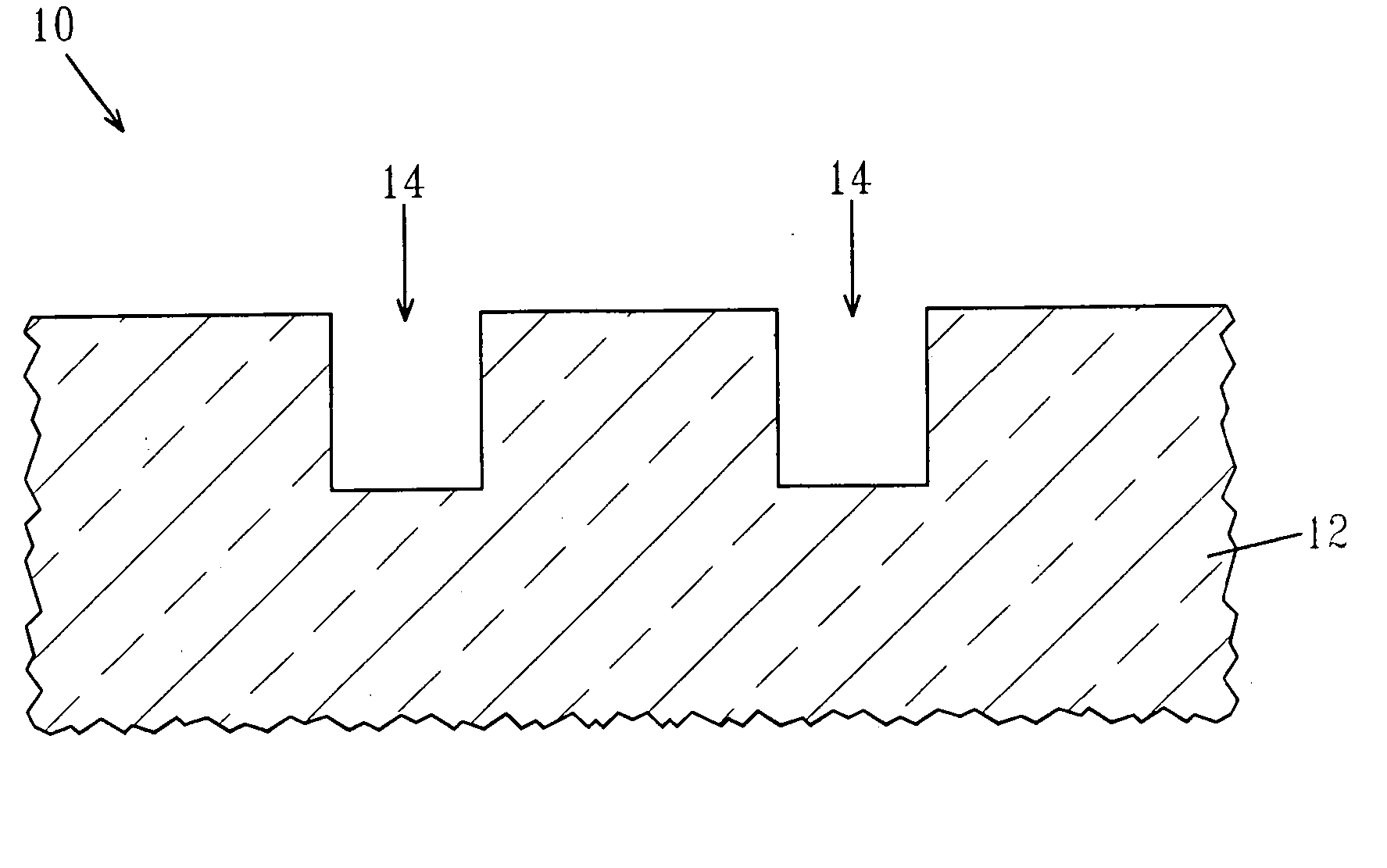
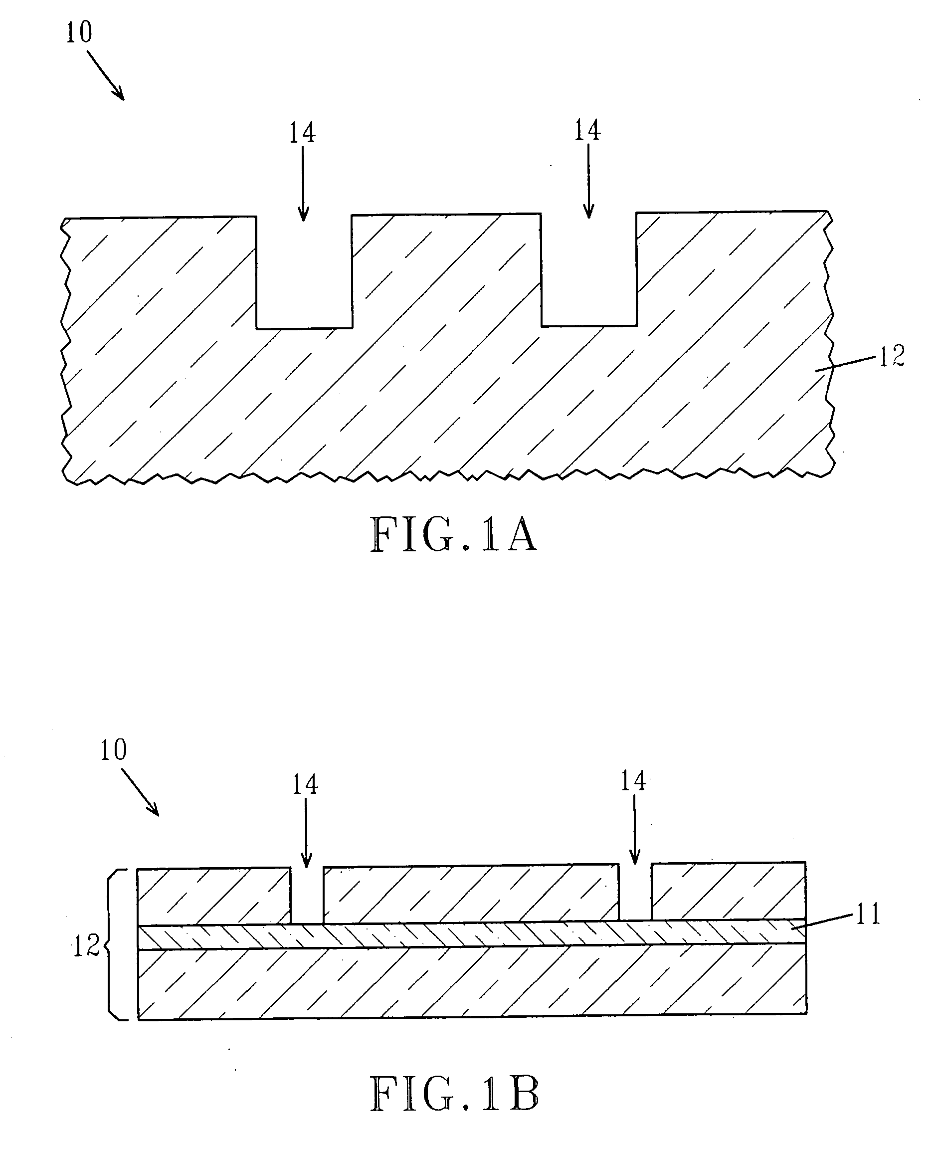
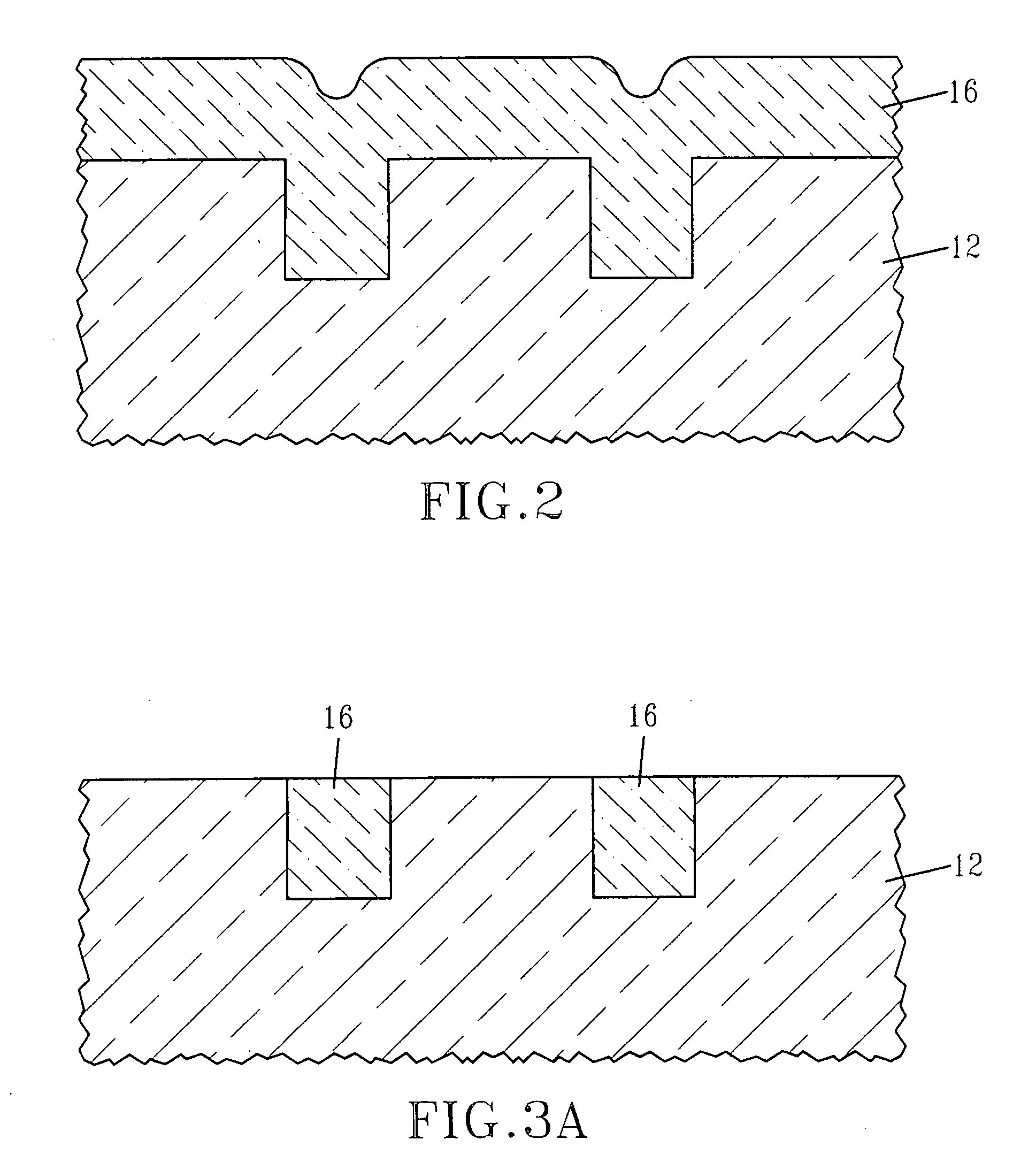
[0028] The present invention, which provides a method for obtaining a free-standing micro structure, will now be described in greater detail by referring to the drawings that accompany the present application. It is noted that the drawings of the present invention are provided for illustrative purposes and thus they are not drawn to scale.

[0029]FIGS. 1-8 describe the inventive process flow and illustrate the material stack used in the creation of a low k film to be released using a combined sacrificial and protective release layer method. The trench dielectric formed into the Si-containing substrate will act as a selective etch-stop for the release process within the Si-containing substrate and will define the area of the released low k film. Alternatively, a Si-containing trench within an insulating region such as a buried oxide region will define the area of the released low k film. In accordance with the present invention, the Si-containing substrate, or sacrificial trench will ...


PUM


Abstract

A method of patterning and releasing chemically sensitive low k films without the complication of a permanent hardmask stack, yielding an unaltered free-standing structure is provided. The method includes providing a structure including a Si-containing substrate having in-laid etch stop layers located therein; forming a chemically sensitive low k film and a protective hardmask having a pattern atop the structure; transferring the pattern to the chemically sensitive low k film to provide an opening that exposes a portion of the Si-containing substrate; and etching the exposed portion of the Si-containing substrate through the opening to provide a cavity in the Si-containing substrate in which a free-standing low k film structure is formed, while removing the hardmask. In accordance with the present invention, the etching comprises a XeF2 etch gas.

Description

FIELD OF THE INVENTION [0001] The present invention relates to semiconductor device fabrication, and more particularly to a method of fabricating a semiconductor structure that includes a free-standing micro structure (or layer). The method of the present invention includes a selective etch process that is capable of removing a protective layer and a sacrificial layer. BACKGROUND OF THE INVENTION [0002] Evaluation of mechanical properties of thin films used in semiconductor processing such as, for example, residual stress, CTE (coefficient of thermal expansion) and Young's modulus, is critical for the understanding of the performance (both mechanical and electrical) of the materials used. As the mechanical properties can significantly vary from wafer to wafer, and with process conditions, obtaining a clear understanding of the effects of processing is very valuable to understanding yield and performance. Currently, the processes in which these films are tested and characterized are ...

Claims


Application Information

Patent Timeline
IPC IPC(8): H01L21/4763
CPCB81B2203/0118B81C1/00476B81C2201/0132G01N1/32Y10S438/933
Inventor COTTE, JOHN MICHAELHOIVIK, NILS DENEKEJAHNES, CHRISTOPHER VINCENT
Owner IBM CORP
Why Eureka
Try Eureka