Method of manufacturing array substrate and method of manufacturing organic EL display device

a technology of organic electroluminescence and array substrate, which is applied in the manufacture of electric discharge tubes/lamps, lighting and heating apparatuses, and tube/lamp factory adjustment. it can solve the problems of display devices that cannot be shipped as a product, display devices that cannot be manufactured with stability, and image quality and display quality greatly decreases

Inactive Publication Date: 2006-08-10
TOSHIBA MATSUSHITA DISPLAY TECH
View PDF6 Cites 25 Cited by
  • Summary
  • Abstract
  • Description
  • Claims
  • Application Information

AI Technical Summary

Benefits of technology

[0012] According to another aspect of the present invention, there is provided a method of manufacturing an organic EL display device, the organic EL display device including an array substrate having a substrate and a plurality of elements arranged on the substrate and having a cathode, an anode opposed to the cathode and an organic active layer interposed between the cathode and the anode, and a sealed substrate which is opposed to one side of the array substrate on which the elements are formed and which makes atmosphere

Problems solved by technology

If a number of pixels are unlit, a display device greatly decreases in image quality and display quality and cannot be shipped a

Method used


Image

  • Method of manufacturing array substrate and method of manufacturing organic EL display device
  • Method of manufacturing array substrate and method of manufacturing organic EL display device
  • Method of manufacturing array substrate and method of manufacturing organic EL display device

Examples


Embodiment Construction

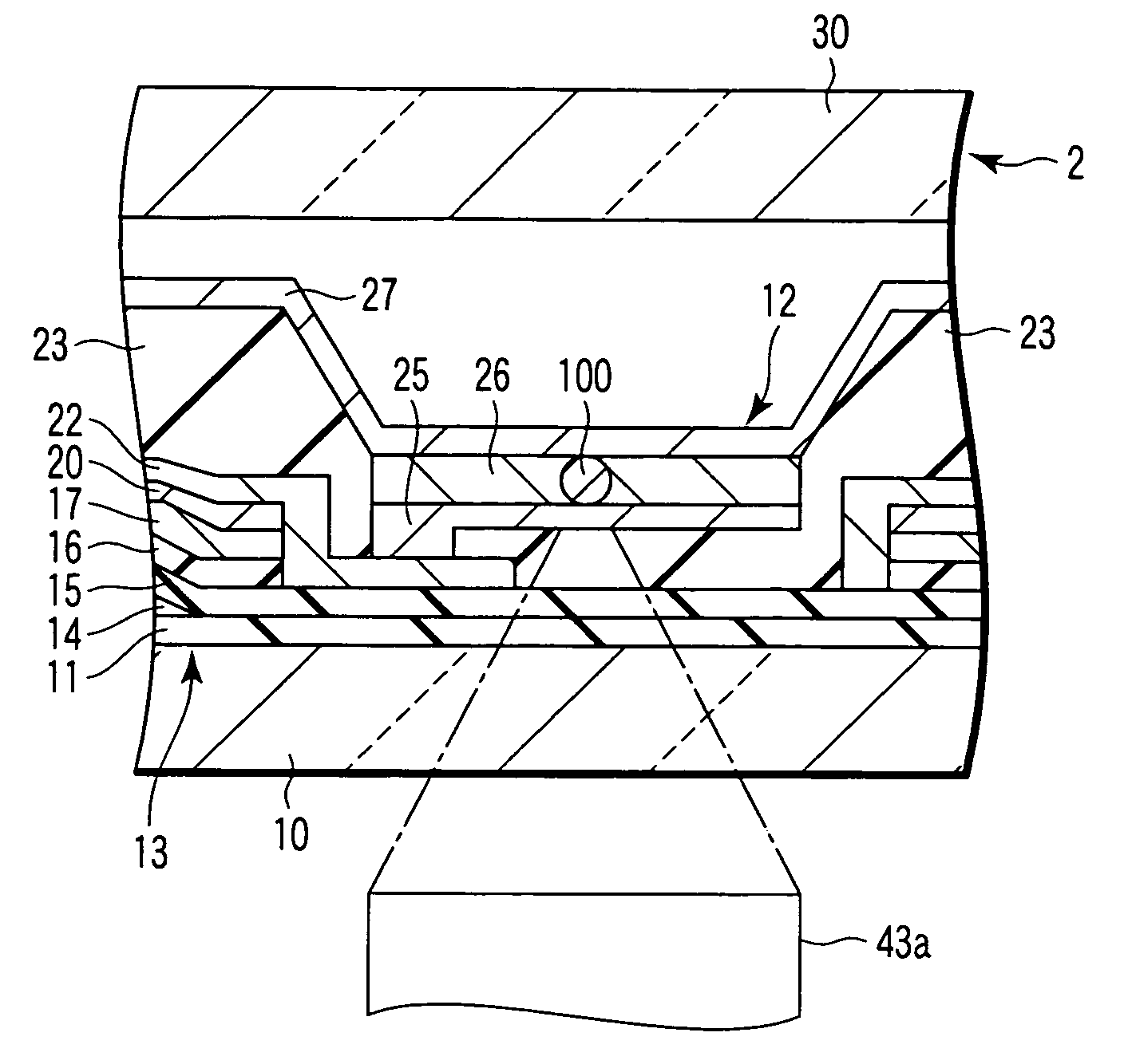
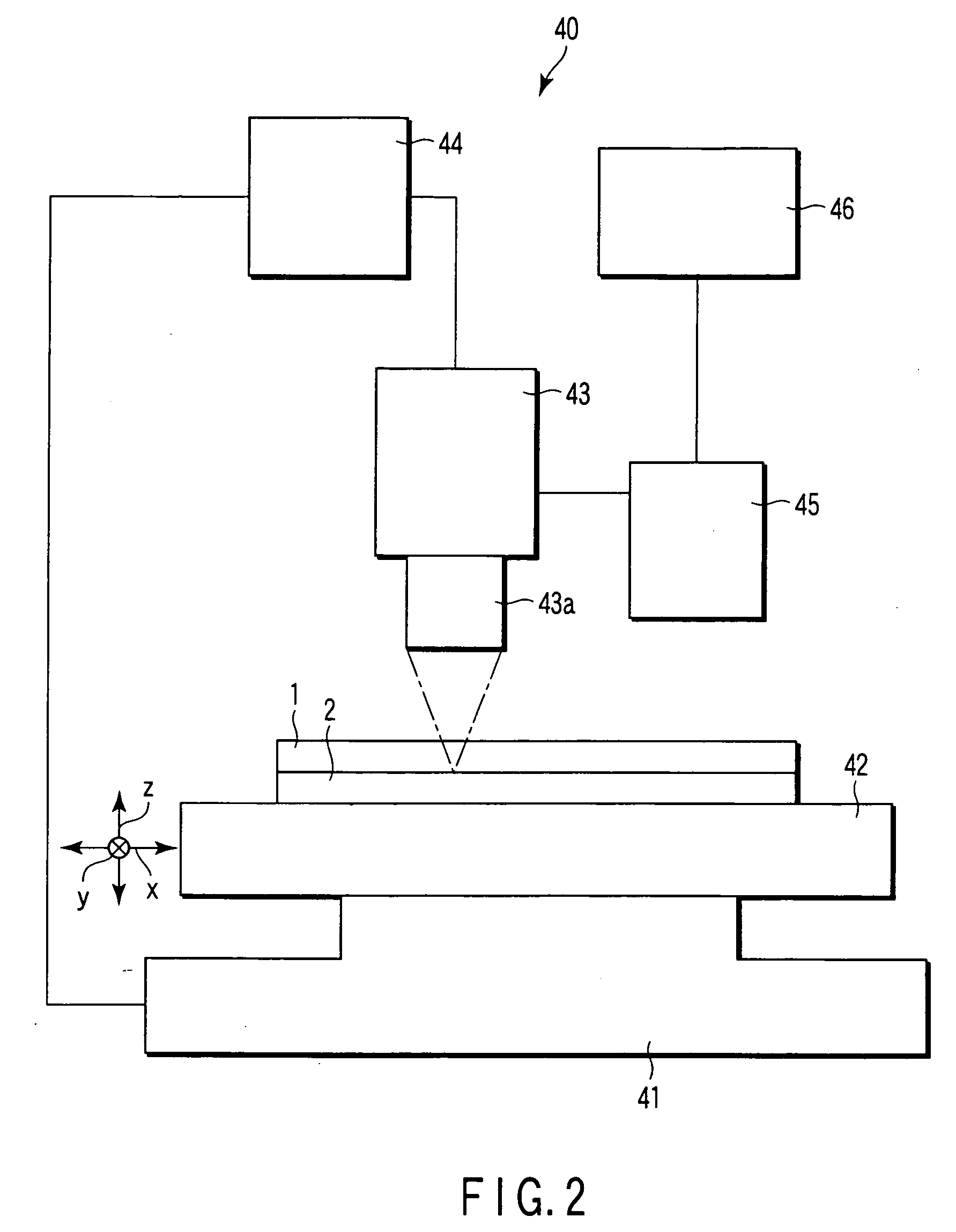
[0023] A method of manufacturing an organic EL display device according to an embodiment of the present invention will be described with reference to the accompanying drawings. First, the configuration of the organic EL display device manufactured by the method will be described.

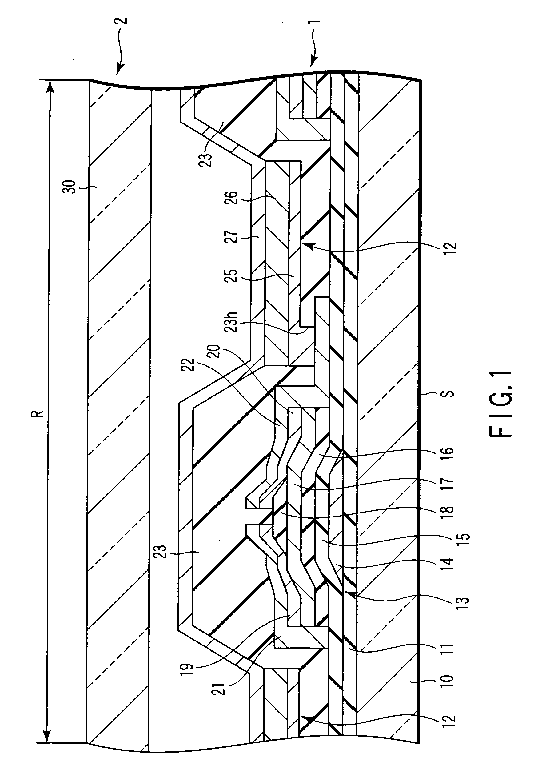
[0024] Referring to FIG. 1, the organic EL display device includes an array substrate 1 having a display surface S and a display region R and a sealed substrate 2 arranged opposite to the array substrate 1 with a given gap therebetween. A seal member (not shown) is provided along the outer edge of the sealed substrate 2. The array substrate 1 and the sealed substrate 2 are stuck to each other by the seal member. The sealed substrate 2 and the seal member make atmosphere between the sealed substrate 2 and seal member and the display region R of array substrate 1 airtight.

[0025] The space surrounded with the display region R of array substrate 1 and the sealed substrate 2 is filled with inert gases such as a...


PUM


Abstract

The size of a foreign substance which is present between a cathode and an anode and which contributes to a short circuit therebetween is measured. On the basis of the measured size, the wavelength of a laser beam with which the foreign substance is irradiated is set, as is the number of times of irradiation. The foreign substance is irradiated with the laser beam to eliminate at least part of the foreign substance.

Description

CROSS-REFERENCE TO RELATED APPLICATIONS [0001] This application is based upon and claims the benefit of priority from prior Japanese Patent Application No. 2005-034810, filed Feb. 10, 2005, the entire contents of which are incorporated herein by reference. BACKGROUND OF THE INVENTION [0002] 1. Field of the Invention [0003] The present invention relates to a method of manufacturing an array substrate and a method of manufacturing an organic electroluminescence (EL) display device having the array substrate. [0004] 2. Description of the Related Art [0005] Recently, for example, an organic EL display device and a liquid crystal display device have been used as a display device. Since the organic EL display device does not require a backlight unit that is used for liquid crystal display devices, it can be thinned, lightened, decreased in power consumption, reduced in costs and achieved as a mercuryless one. Since, moreover, it is a self-luminous display device, it has the features of wi...

Claims


Application Information

Patent Timeline
IPC IPC(8): H01J9/44
CPCH01L27/3244H01L51/56H01L2251/568H10K59/12H10K71/861H10K71/00
Inventor KONDA, NOBUO
Owner TOSHIBA MATSUSHITA DISPLAY TECH
Why Eureka
Try Eureka