Multilayer printed wiring board and process for producing the same

a wiring board and multi-layer technology, applied in the direction of printed circuit manufacturing, printed circuit aspects, semiconductor/solid-state device details, etc., can solve the problems of wasteful material costs, little design freedom for wiring, and assembling processes of rigid portions on inner and outer layer rigid substrates. achieve the effect of reducing material costs, reducing substrate capacity, and high wiring design freedom

Inactive Publication Date: 2006-08-17
THE FUJIKURA CABLE WORKS LTD
View PDF2 Cites 101 Cited by
  • Summary
  • Abstract
  • Description
  • Claims
  • Application Information

AI Technical Summary

Benefits of technology

[0012] The present invention has been devised to solve the above-mentioned problems, and the first objective thereof is to provide a multi-layer wiring board which provides higher design freedom for wiring, and makes it possible to cut material costs, and also to reduce the substrate capacity, and a manufacturing method for such a wiring board.

Problems solved by technology

In other words, in the conventional rigid flex printed circuit board, since the rigid portion needs to be laminated at a predetermined position of the flex substrate, assembling processes of the rigid portions on the inner layer and outer layer rigid substrates, which are carried out so as to place the rigid portions at predetermined positions on the flex substrate when formed as laminated layers, are limited by factors such as an outer shape and positions of the flex substrate.
For this reason, excessive multi-layered areas exist on the rigid portion, causing wasteful material costs.
Further, there is a limitation in positions in which multi-layered areas are placed, resulting in little design freedom for wiring.

Method used


Image

  • Multilayer printed wiring board and process for producing the same
  • Multilayer printed wiring board and process for producing the same
  • Multilayer printed wiring board and process for producing the same

Examples


first embodiment

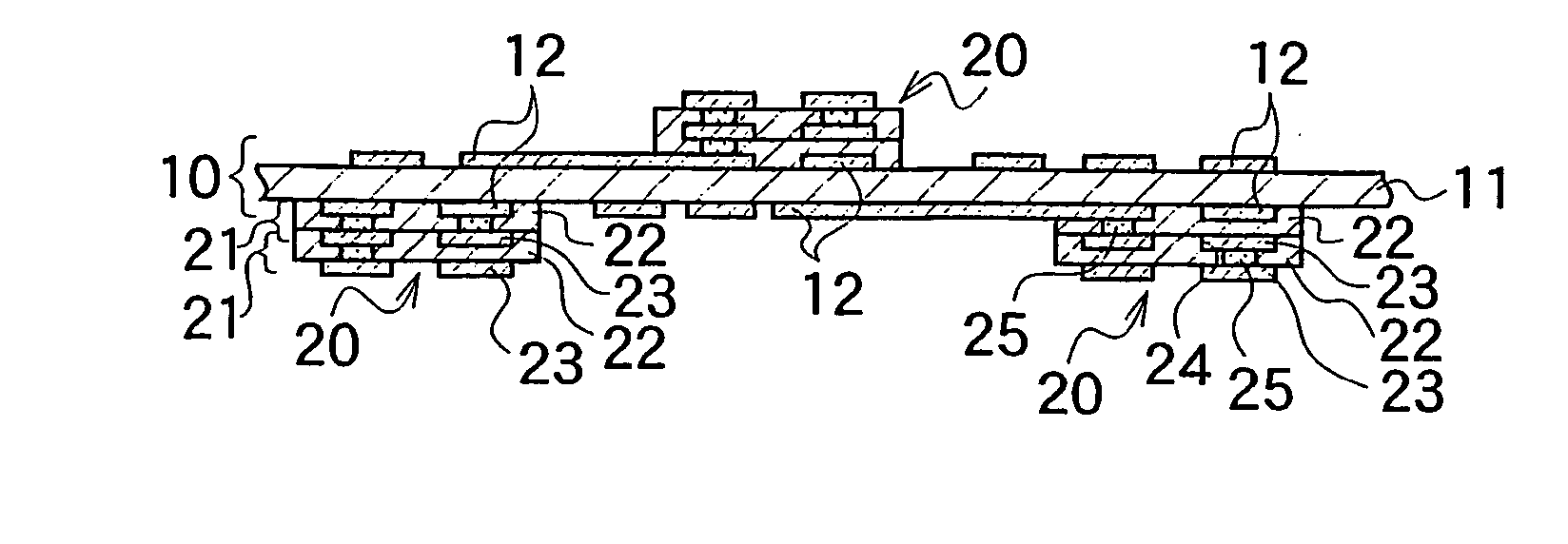
[0064]FIGS. 3 and 4 show a basic mode of a multi-layer wiring board in accordance with a first embodiment of the present invention. In the multi-layer wiring board of the present embodiment, at a plurality of portions on the surface and rear surface of a motherboard (base material) 10, partial wiring boards (multi-layer portions) 20, which have outer shapes that have been preliminarily formed into predetermined shapes, and will be described later, are bonded so as to form an island shape. Here, the island shape is defined as a state in which the peripheral sides of the partial wiring boards 20 are not coincident with the peripheral sides of the motherboard 10 so that the partial wiring boards 20 are placed inside the area which is defined by the peripheral sides of the motherboard 10. Additionally, the predetermined shapes are determined on the request of designing the motherboard.

[0065] The partial wiring boards 20 are formed as follows: a plurality of resin base materials 21 with...

first embodiment-second modified embodiment

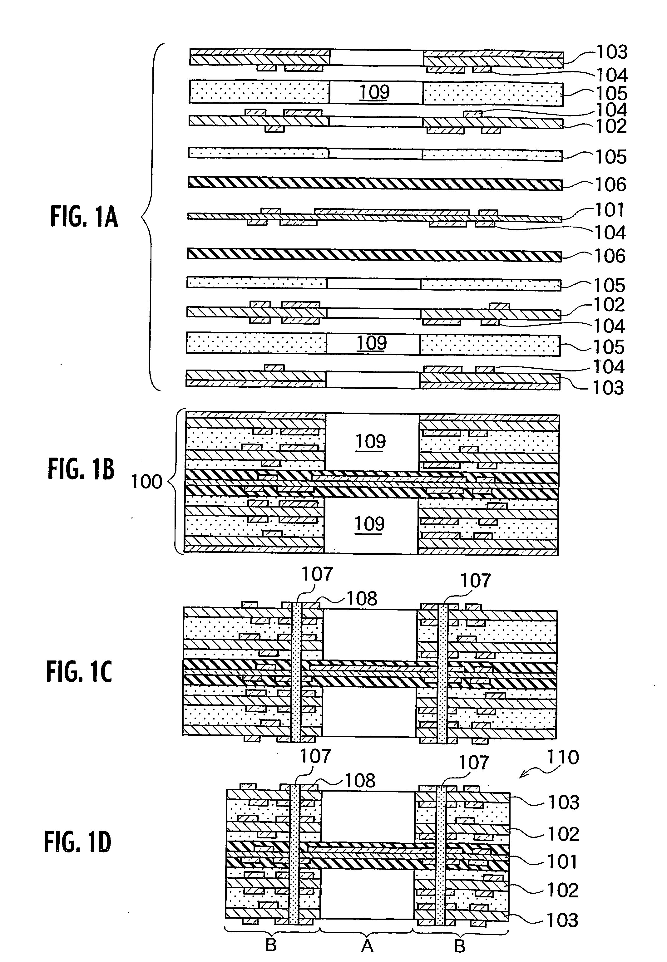
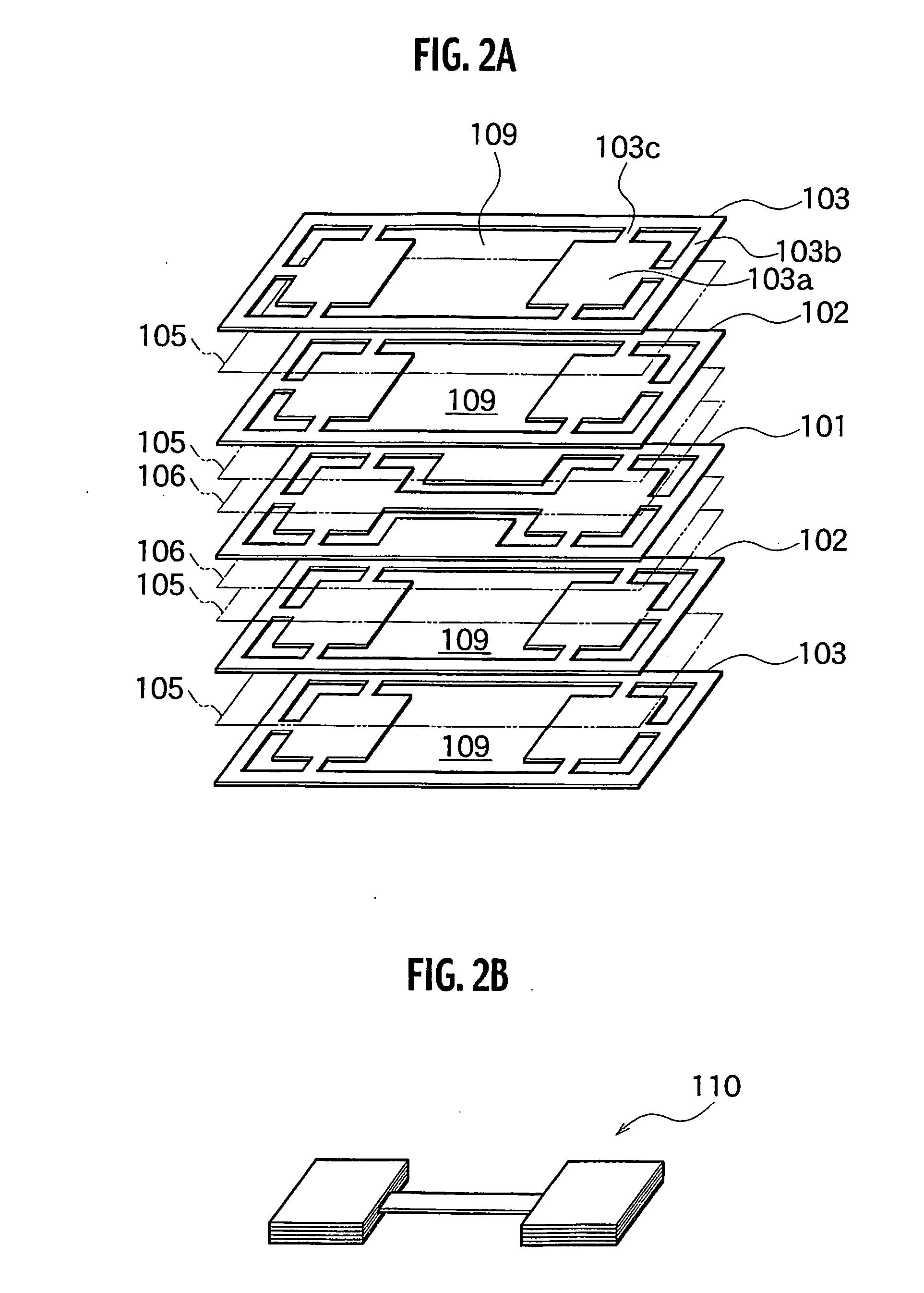
[0096] Referring to FIGS. 14A to 14E, a manufacturing method for a multi-layer wiring board in accordance with a second modified embodiment of the first embodiment will be described below. Here, in FIG. 14 also, those parts corresponding to those shown in FIG. 12 are indicated by the same reference numerals as those of FIG. 12 and the description thereof is omitted.

[0097] As shown in FIG. 14A, a motherboard FPC 60 has a wiring circuit 61 formed thereon and is provided with a cover layer 62 with openings (opening sections 62A and 62B) formed at portions to receive laminated layers that is formed on the surface thereof. Two layers of resin base materials 57 with single-sided wiring circuits that have an outer shape that has been formed into a predetermined shape, as shown in FIG. 9, are positioned, and then superposed thereon. Thereafter, these members are subjected to heating and pressing processes by a vacuum heat pressing machine under a degree of vacuum of not more than 1 kPa so ...

second embodiment

[0101] With reference to attached Figures, a second embodiment of the present invention will be described below.

[0102]FIGS. 15 and 16 show a second embodiment of a multi-layer wiring board in accordance with the present invention.

[0103] In the multi-layer wiring board of the present embodiment, at a plurality of portions on the surface and rear surface of a motherboard (base material) 210, partial wiring boards (multi-layer portions) 220, which have outer shapes that have been preliminarily formed into predetermined shapes, are bonded so as to form an island shape. Here, the island shape is defined as a state in which the peripheral sides of the partial wiring boards 220 are not coincident with the peripheral sides of the motherboard 210 so that the partial wiring boards 220 are placed inside the area determined by the peripheral sides of the motherboard 210. Here, the predetermined shapes are determined by requirements in designing the motherboard.

[0104] The partial wiring board...


PUM

PropertyMeasurementUnit
elastic modulusaaaaaaaaaa
glass transition temperatureaaaaaaaaaa
thicknessaaaaaaaaaa

Abstract

At least one base material having a wiring circuit that has been formed into a predetermined outer shape is bonded to a motherboard. The motherboard wiring board and the base material having a wiring circuit are electrically connected to each other at least one portion through an inner via hole. The outer shape of the base material having a wiring circuit is smaller than the outer shape of the motherboard, with the base material having a wiring circuit having an island shape on the motherboard.

Description

TECHNICAL FIELD [0001] The present invention relates to a multi-layer wiring board and a method for manufacturing the same. BACKGROUND ART [0002] Recent electronic apparatuses have been made smaller and light weight in addition to developments in the applicability to high-frequency signals and digitized devices, and along with these developments, there have been demands for small-size devices, a high-density packaging property and the like in printed circuit boards being installed in the electronic apparatuses. [0003] There is a rigid flex printed circuit board satisfying these demands which includes a rigid portion and a flex portion (for example, Japanese Patent Application Laid Open Publication No. 2002-158445). [0004] With reference to FIGS. 1A to 2B, a manufacturing process of a conventional rigid flex printed circuit board will be described bellow. FIGS. 1A to 1D are flow charts that show manufacturing processes of the rigid flex printed circuit board. FIG. 2A is a perspective...

Claims


Application Information

Patent Timeline
Patent Type & Authority Applications(United States)
IPC IPC(8): H05K1/11H05K1/09H05K1/03H01L23/538H05K3/46
CPCH01L23/5385H01L2224/16H01L2924/01078H01L2924/01079H01L2924/3511H05K3/4602Y10T29/49165H05K3/4691H05K3/4694H05K2201/09972H01L2924/01068Y10T29/4916Y10T29/49128H05K3/4614H01L2924/00011H01L2924/00014H01L2924/1627H01L2224/0401
Inventor ITO, SHOJIKISHIHARA, RYOICHINAKAO, OSAMUHASHIBA, HIROKIOKAMOTO, MASAHIRO
Owner THE FUJIKURA CABLE WORKS LTD
Why Eureka
Try Eureka