

Structure and method for manufacturing strained finfet
a technology of metal oxide semiconductor and finfet, which is applied in the direction of transistors, semiconductor devices, electrical equipment, etc., can solve the problems of difficult to apply a large stress in the channel of a finfet, difficult to contact the source and drain regions, etc., to achieve the effect of improving the performance of the finfet, stressing the channel, and enhancing electron and hole mobility
- Summary
- Abstract
- Description
- Claims
- Application Information
AI Technical Summary
Benefits of technology
Problems solved by technology
Method used
Image

Examples
Embodiment Construction
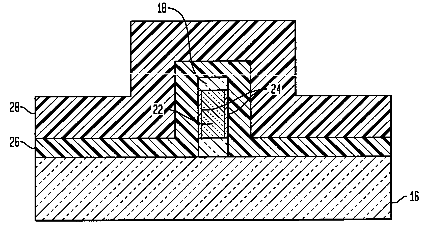
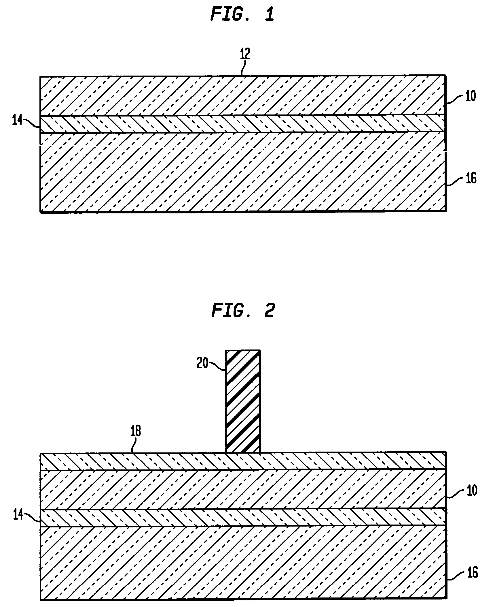
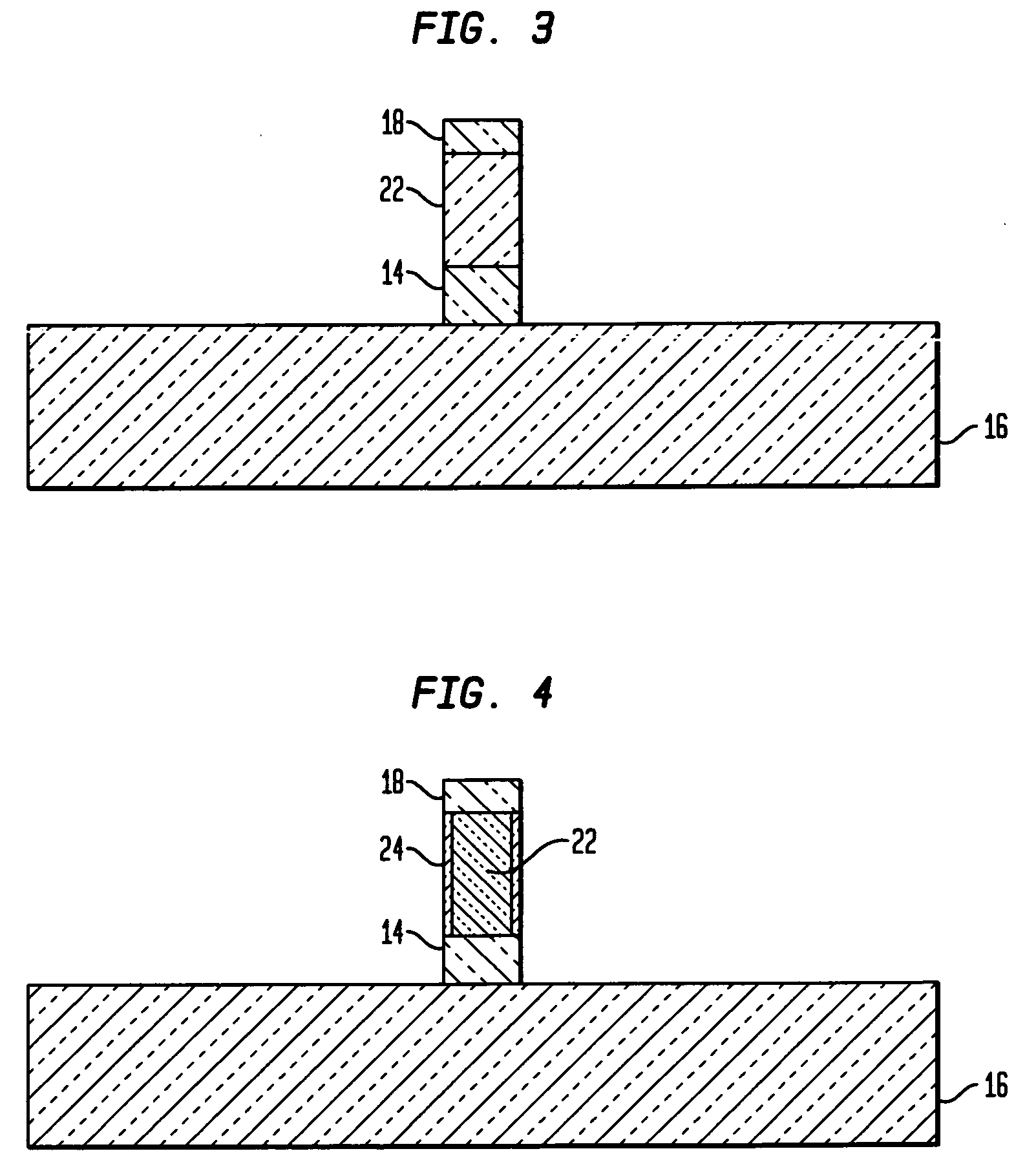
[0024] Stress can enhance electron and hole mobility, but it is difficult to apply a large stress in the channel of a FINFET device. The present invention replaces a part of the gate of a FINFET with a stress material to apply stress to the channel of the FINFET to enhance electron and hole mobility and improve performance of the FINFET. More particularly, the present invention replaces the SiGe part of a SiGe / Si stacked gate of a FINFET with a stress nitride film to apply stress to the channel of the FINFET to enhance electron and hole mobility and improve performance of the FINFET.
[0025] In general, the present invention uses a SiGe / Si stacked gate to replace a poly-Si gate. Before silicidation, selectively etch the SiGe part of the gate to make the gate thin enough to be fully silicided. After silicidation and etching of residual metal, refill the gate-gap with stress nitride film. This creates stress in the channel and enhances the performance of the FINFET. Other process steps...
PUM
 Abstract
Description
Claims
Application Information