Tamper-resistant semiconductor device
a semiconductor device and resistance technology, applied in the direction of logic circuits, semiconductor/solid-state device details, pulse techniques, etc., can solve the problem of significant increase in the difficulty of machining, and achieve the effect of high tamper resistan
- Summary
- Abstract
- Description
- Claims
- Application Information
AI Technical Summary
Benefits of technology
Problems solved by technology
Method used
Image

Examples
embodiment 1
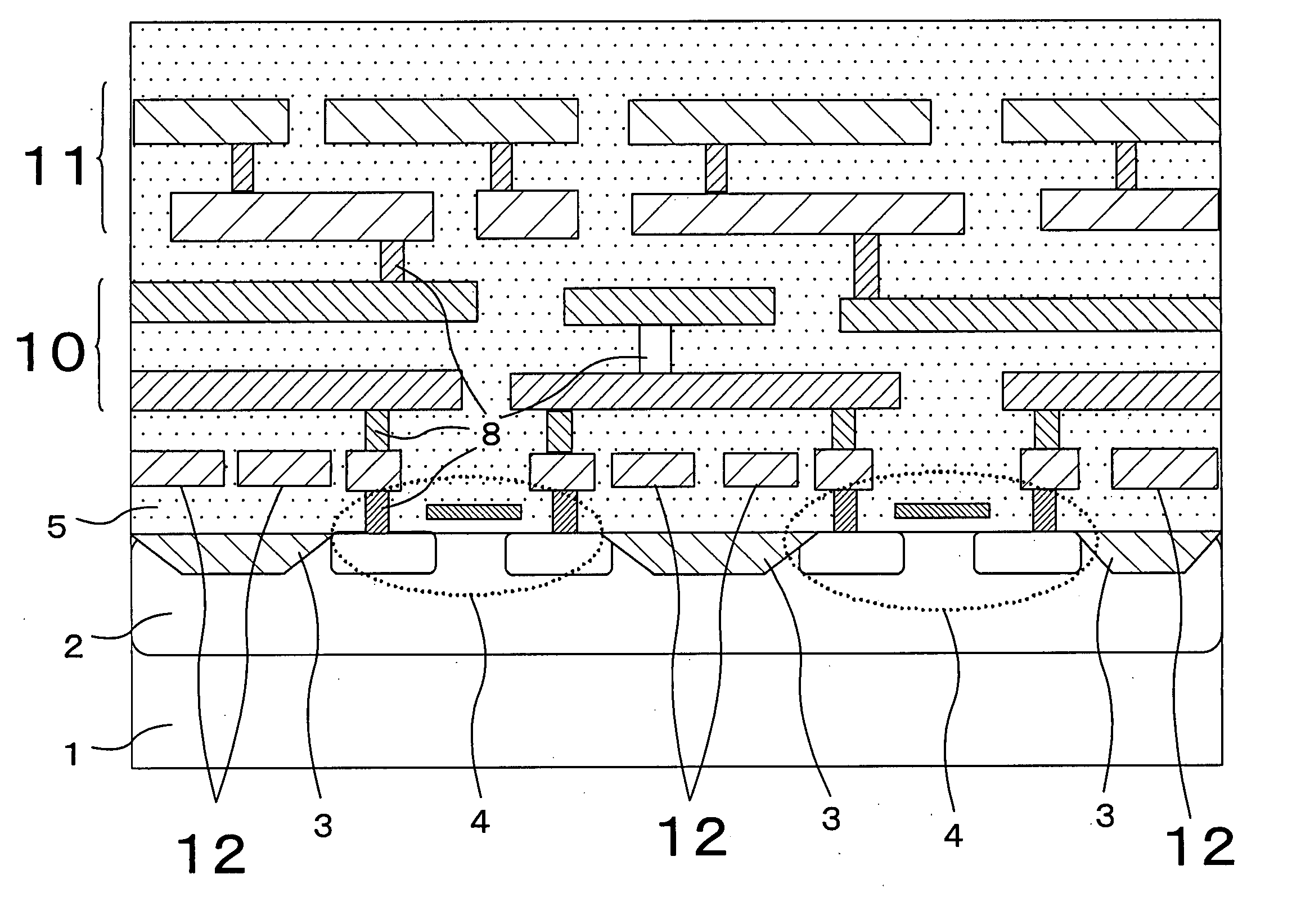
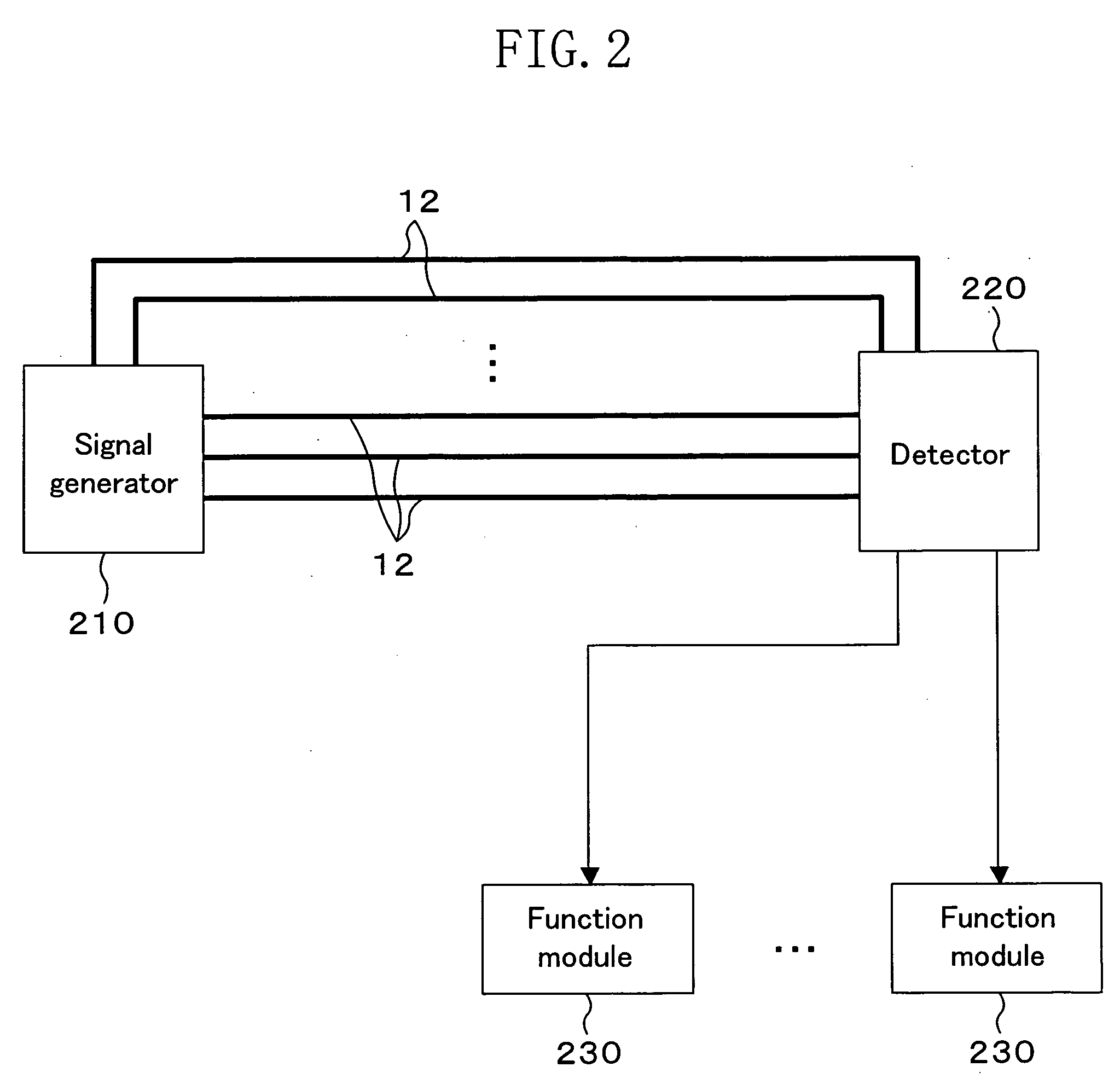
[0041]FIG. 1 shows a cross-sectional structure of a semiconductor device of Embodiment 1 of the present invention. The semiconductor device has transistor elements 4 formed on a p- or n-well 2 that is formed on a semiconductor substrate (p- or n-substrate) 1. A diffusion isolation layer 3 is formed between every adjacent transistor elements 4. Defense wiring 12 is placed above the diffusion isolation layer 3. The defensive wiring 12, which is formed from a lowermost wiring layer, is arranged to cover the region above the diffusion isolation layer 3 at the minimum wiring pitch allowable in fabrication. Above the wiring layer forming the defensive wiring 12, a signal wiring layer 10 is placed, from which signal wiring requiring secrecy (for example, data lines of a memory) is formed. A signal wiring layer 11, from which signal wiring requiring no secrecy (for example, control signal lines on a chip), is placed above the signal wiring layer 10. The signal wiring of the signal wiring la...
application of embodiment 1
[0047]FIG. 3 shows a cross-sectional structure of a semiconductor device of an application of Embodiment 1. The semiconductor device of FIG. 3 has the same structure as the semiconductor device of Embodiment 1 (FIG. 1), except that defensive wiring 20 is formed from a polysilicon layer used for formation of the gates of the MOS transistors 4. This structure makes it unnecessary to newly provide a wiring layer dedicated to the defensive wiring 20, and thus the number of fabrication steps and the fabrication cost can be reduced.
embodiment 2
[0048]FIG. 4 shows a cross-sectional structure of a semiconductor device of Embodiment 2 of the present invention. The semiconductor device of FIG. 4 has the same multilayer wiring structure as that in Embodiment 1 against an attempt of fraudulent analysis from the front, but is provided with a barrier diffused layer 30 against an attempt of fraudulent analysis from the back, in place of the defensive wiring 12. The barrier diffused layer 30 is formed on the p- or n-well 2 with the minimum gap allowable in fabrication from the adjacent diffused layer of the transistor element formation portion 4, and has the polarity (conductivity) opposite to that of the p- or n-well 2. The barrier diffused layer 30 is also applied with a potential reverse-biased to that of the p- or n-well 2. For example, when the potential of the p- or n-well 2 is VSS, the potential VDD is applied to the barrier diffused layer 30, and vice versa.
[0049] The semiconductor device of this embodiment has the same tam...
PUM
 Abstract
Description
Claims
Application Information
 - R&D
- Intellectual Property
- Life Sciences
- Materials
- Tech Scout
- Unparalleled Data Quality
- Higher Quality Content
- 60% Fewer Hallucinations
Browse by: Latest US Patents, China's latest patents, Technical Efficacy Thesaurus, Application Domain, Technology Topic, Popular Technical Reports.
© 2025 PatSnap. All rights reserved.Legal|Privacy policy|Modern Slavery Act Transparency Statement|Sitemap|About US| Contact US: help@patsnap.com