Camera module

a technology of camera modules and modules, applied in the field of camera modules, can solve the problems of reducing affecting the focusing arrangement the number of components of the camera module is large, so as to reduce the manufacturing cost of the camera module, simplify the structure, and improve the productivity of the camera module

Inactive Publication Date: 2006-08-17
SAMSUNG ELECTRO MECHANICS CO LTD
View PDF3 Cites 102 Cited by
  • Summary
  • Abstract
  • Description
  • Claims
  • Application Information

AI Technical Summary

Benefits of technology

[0017] Therefore, the present invention has been made in view of the above problems, and it is an object of the present invention to provide a camera module having a structure for preventing injurious electromagnetic waves generated in the camera module from being emitted out of the camera module and preventing external injurious electromagnetic waves from being introduced into the camera module, wherein the structure is simplified without using additional parts, whereby productivity of the camera module is improved, the manufacturing costs of the camera module are reduced, and the size of the camera module is decreased.
[0018] In accordance with one aspect of the present invention, the above and other objects can be accomplished by the provision of a camera module comprising: a lens array including at least one lens; a lens accommodating unit having an inner space defined therein such that the lens array is arranged along an optical axis in the inner space and an incident hole formed at the center of the front surface thereof; a housing mounted on the upper surface of a circuit board, the housing having a counter-engagement part engaged with an engagement part formed at the lens accommodating unit such that the lens accommodating unit is moved in the direction of the optical axis; an image sensor having an image area on which light passing through the lens array is focused, the image sensor being electrically connected to the circuit board such that the image focused on the image area is transmitted to the circuit board; and a filter disposed between the lens array and the image sensor, the filter including a transparent medium through which light introduced along the optical axis is directly transmitted to the image area of the image sensor, and a prevention film for preventing electromagnetic waves generated by the image sensor disposed in the housing from being emitted out of the housing.
[0029] In accordance with another aspect of the present invention, there is provided a camera module comprising: a lens array including at least one lens; a lens accommodating unit having an inner space defined therein such that the lens array is arranged along an optical axis in the inner space and an incident hole formed at the center of the front surface thereof; a housing mounted on the upper surface of a circuit board such that the housing is connected to at least one ground terminal of the circuit board, the housing having a counter-engagement part engaged with an engagement part formed at the lens accommodating unit such that the lens accommodating unit is moved in the direction of the optical axis; an image sensor having an image area on which light passing through the lens array is focused, the image sensor being electrically connected to the circuit board such that the image focused on the image area is transmitted to the circuit board; and a filter disposed between the lens array and the image sensor, the filter including a transparent medium through which light introduced along the optical axis is directly transmitted to the image area of the image sensor, and a prevention film for preventing electromagnetic waves generated by the image sensor disposed in the- housing from being emitted out of the housing.

Problems solved by technology

As a result, the number of components of the camera module is large, and the assembly process is complicated, which deteriorates productivity of the camera module.
Furthermore, it is difficult to decrease the size of the camera module according to demand for miniaturization.

Method used


Image

  • Camera module
  • Camera module
  • Camera module

Examples


Embodiment Construction

[0052] Now, preferred embodiments of the present invention will be described in detail with reference to the accompanying drawings.

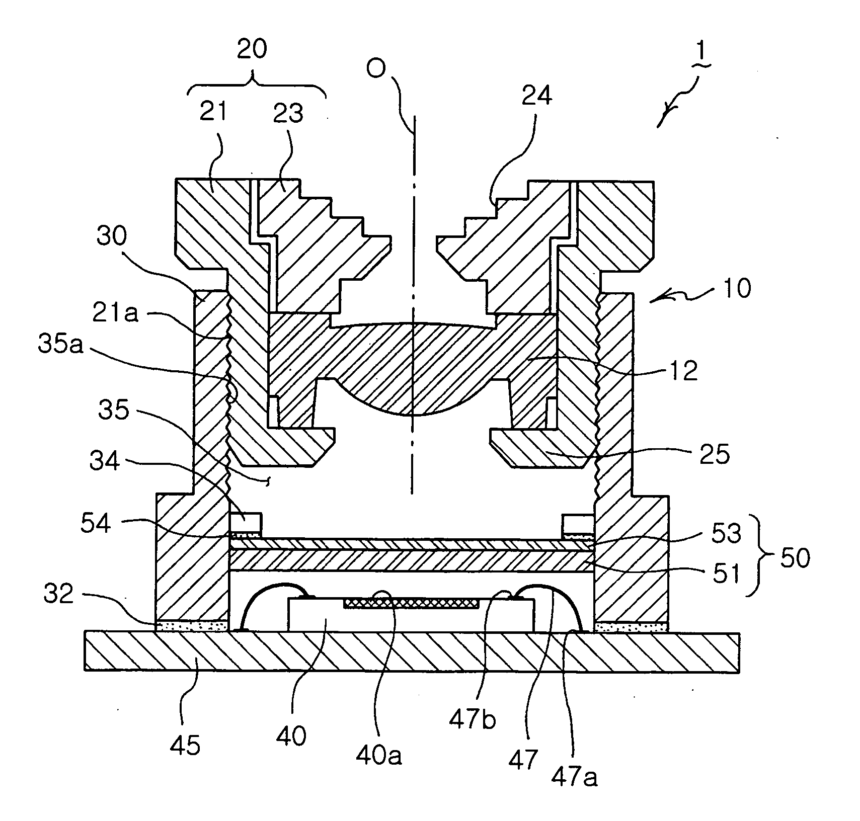
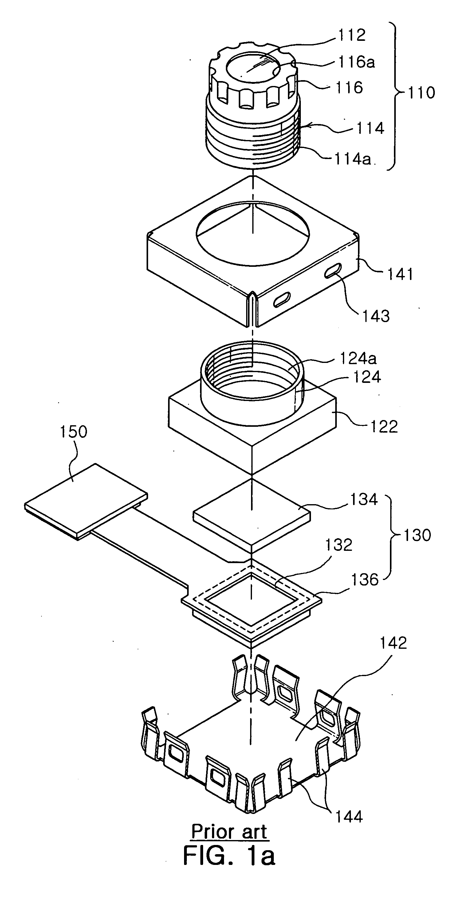
[0053]FIG. 2a is an exploded perspective view illustrating a camera module 1 according to a first preferred embodiment of the present invention, and FIG. 2b is an assembled sectional view illustrating the camera module 1 according to the first preferred embodiment of the present invention.

[0054] As shown in FIGS. 2a and 2b, the camera module 1 according to the first preferred embodiment of the present invention comprises a lens array 10, a lens accommodating unit 20, a housing 30, an image sensor 40, and a filter 50.

[0055] The lens array 10 includes at least one lens 12 arranged along the optical axis O and disposed in the lens accommodating unit 20.

[0056] Preferably, a plurality of lenses 12 may be arranged in the lens accommodating unit 20. In this case, spacers are disposed between the respective lenses 12 such that the lenses 12 are spaced unifor...


PUM


Abstract

A camera module comprises a lens array including at least one lens, a lens accommodating unit having an inner space, in which the lens array is arranged, and an incident hole, and a housing mounted on a circuit board. The housing has a counter-engagement part engaged with an engagement part formed at the lens accommodating unit such that the lens accommodating unit is moved in the direction of the optical axis. An image sensor has an image area on which light is focused. The image sensor is electrically connected to the circuit board. A filter is disposed between the lens array and the image sensor. The filter includes a transparent medium through which light introduced along the optical axis is transmitted to the image area, and a prevention film for preventing electromagnetic waves generated by the image sensor from being emitted out of the housing.

Description

RELATED APPLICATIONS [0001] The present application is based on, and claims priority from, Korean Application Number 2005-12674, filed Feb. 16, 2005, the disclosure of which is incorporated by reference herein in its entirety. BACKGROUND OF THE INVENTION [0002] 1. Field of the Invention [0003] The present invention relates to a camera module, and, more particularly to a camera module having a structure for preventing electromagnetic waves generated in the camera module from being emitted out of the camera module and preventing external electromagnetic waves and noise from being introduced into the camera module, wherein the structure is simplified without using additional parts, whereby assembly of the camera module is improved, the manufacturing costs of the camera module are reduced, and the size of the camera module is decreased. [0004] 2. Description of the Related Art [0005] Generally, a camera module comprises a lens unit including at least one lens, a housing in which the len...

Claims


Application Information

Patent Timeline
Patent Type & Authority Applications(United States)
IPC IPC(8): H04N5/225G02B7/02G03B11/00G03B17/02H04N5/335
CPCH04N5/2251H04N5/2253H04N5/2254G02B7/02H04N23/54H04N23/55G02B7/025G02B7/022H04N23/51
Inventor SEO, TAE JUN
Owner SAMSUNG ELECTRO MECHANICS CO LTD
Why Eureka
Try Eureka