Thermally coupled surfaces having controlled minimum clearance

a technology of thermal coupling and minimum clearance, which is applied in the direction of cooling/ventilation/heating modification, semiconductor/solid-state device details, semiconductor devices, etc., can solve the problems of increasing power density, reducing the total contact area between the two, and limiting the ability to adequately cool these chips. , to achieve the effect of reducing the total contact area between

Inactive Publication Date: 2006-08-24
THERMAL
View PDF22 Cites 18 Cited by
  • Summary
  • Abstract
  • Description
  • Claims
  • Application Information

AI Technical Summary

Problems solved by technology

As IC chip geometries are scaled down and operating speeds are increased, the resulting increase in power density exacerbates the problem of heat removal.
Thus, the ability to adequately cool these chips has become a limiting factor to increased system performance.
Gaps between the source and sink (e.g. due to surface discontinuities, defects, etc.), reduce the total contact area between the surfaces, which in turn reduces the area available for conductive heat transfer between the components.
Another important concern when employing metal heat sink components to cool IC chips is the danger of causing an electrical short in the chip or its connections due to the conduction of electric

Method used


Image

  • Thermally coupled surfaces having controlled minimum clearance
  • Thermally coupled surfaces having controlled minimum clearance
  • Thermally coupled surfaces having controlled minimum clearance

Examples


Embodiment Construction

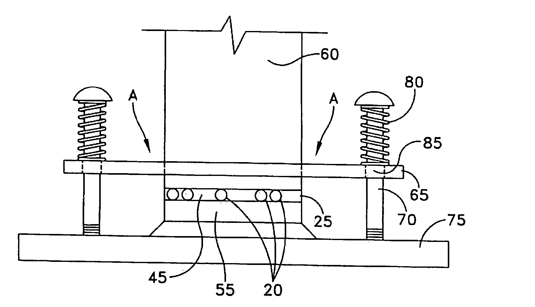
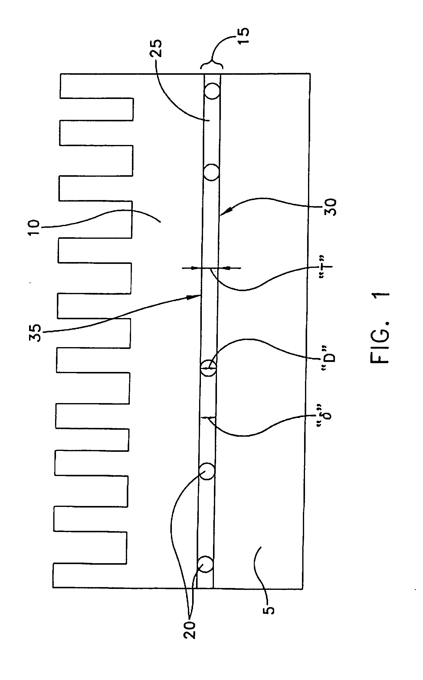
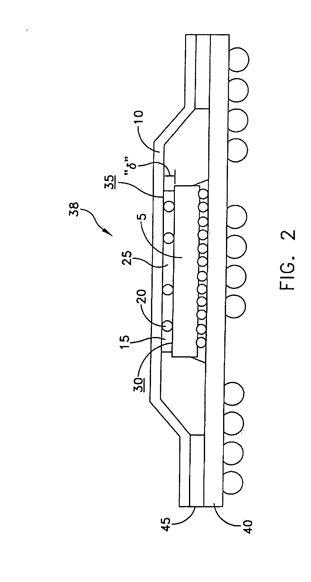
[0014] This description of preferred embodiments is intended to be read in connection with the accompanying drawings, which are to be considered part of the entire written description of this invention. The drawing figures are not necessarily to scale and certain features of the invention may be shown exaggerated in scale or in somewhat schematic form in the interest of clarity and conciseness. In the description, relative terms such as “horizontal,”“vertical,”“up,”“down,”“top” and “bottom” as well as derivatives thereof (e.g., “horizontally,”“downwardly,”“upwardly,” etc.) should be construed to refer to the orientation as then described or as shown in the drawing figure under discussion. These relative terms are for convenience of description and normally are not intended to require a particular orientation. Terms including “inwardly” versus “outwardly,”“longitudinal” versus “lateral” and the like are to be interpreted relative to one another or relative to an axis of elongation, o...


PUM


Abstract

A conformable, thermally conductive layer is provided comprising a flowable component and a plurality of substantially incompressible spacer particles, wherein the conductive layer is disposed between a pair of heat exchange surfaces of an electronic device to maintain a desired spacing during operation. The thermally conductive layer enhances heat transfer between the surfaces while the spacer layer ensures a constant desired offset between the surfaces both to maintain an optimum level of heat transfer and to provide a desired voltage standoff between the surfaces to prevent arcing across the surfaces. The offset is substantially equal to the diameter of the spacer particles, and the particles align in a single layer between the heat exchange surfaces. The heat exchange surfaces can be a heat source such as an integrated circuit chip, and the heat sink can be a plate with a plurality of fins. The flowable component can be a thermal grease or paste, and the spacer particles can be ceramic or glass material. A method of applying the conductive layer and of assembling the heat source and heat sink is also disclosed.

Description

FIELD OF THE INVENTION [0001] This invention deals generally with thermally conductive, electrically insulating interface layers for coupling heat sinks to semiconductor chips or other electrical devices. BACKGROUND OF THE INVENTION [0002] Heat removal from integrated circuits (ICs, or “chips”) has long been an important design consideration because of the need to maintain the components at a sufficiently low operating temperature to ensure continued device reliability. As IC chip geometries are scaled down and operating speeds are increased, the resulting increase in power density exacerbates the problem of heat removal. Thus, the ability to adequately cool these chips has become a limiting factor to increased system performance. Common techniques for removing heat from high-power ICs make use of a cooling device (e.g. heat sink fin or plates, etc.) which is operatively connected to the chip. Heat may be dissipated from the cooling device using a variety of methods, including force...

Claims


Application Information

Patent Timeline
IPC IPC(8): H05K7/20
CPCH01L23/36H01L23/3733H01L23/40H01L2224/16H01L2224/73253H01L2924/09701H01L2924/15311H01L2924/16152H01L2924/00011H01L2924/00014H01L2224/0401
Inventor GARNER, SCOTT
Owner THERMAL
Why Eureka
Try Eureka