Photoelectric converting layer lamination type solid-state image pick-up device

a photoelectric and lamination technology, applied in the direction of radio frequency controlled devices, instruments, television systems, etc., can solve the problems of poor manufacturing yield, small upper limit of optical charges stored in one light receiving portion which is microfabricated, and progress of ccd type image sensor and cmos type image sensor techniques to an almost limit, so as to avoid the generation of shading

Inactive Publication Date: 2006-08-24
FUJIFILM CORP
View PDF1 Cites 18 Cited by
  • Summary
  • Abstract
  • Description
  • Claims
  • Application Information

AI Technical Summary

Benefits of technology

[0020] It is an object of the invention to provide a photoelectric converting layer lamination type solid-state image pick-up device capable of increasing a pixel separation performance of a detection signal to enhance S / N and suppressing a difference in a sensitivity for each color to improve picture quality, and furthermore, preventing shading from being generated.
[0022] By this structure, a pixel separation performance of an image signal (a detection signal) detected from each pixel can be improved and S / N of the detection signal can be enhanced.
[0024] By this structure, the sensitivities of a layer for photoelectrically converting a red light, a layer for photoelectrically converting a green light and a layer for photoelectrically converting a blue light can be made uniform in each pixel so that a difference in the sensitivity for each color is eliminated. Consequently, it is possible to pick up a color image having a high color balance and high picture quality.
[0026] By this structure, it is possible to avoid the generation of shading.

Problems solved by technology

However, the techniques of the CCD type image sensor and the CMOS type image sensor have progressed to an almost limit and a size of an opening of one light receiving portion has been close to a wavelength order of an incident light, that is, approximately 2 μm.
For this reason, they have been confronted with a problem in that a manufacturing yield is poor.
Moreover, an upper limit of a quantity of optical charges stored in one light receiving portion which is microfabricated is small, that is, approximately 3000 electrons.
Consequently, it has also been difficult to finely represent 256 gradations.
For this reason, it has been hard to expect a more excellent image sensor of a CCD type or a CMOS type in respect of picture quality or a sensitivity.
In the related-art photoelectric converting layer lamination type solid-state image pick-up device shown in FIG. 5, there is a problem in that a difference in a sensitivity for each color is made and a color balance of a pick-up image is thus lost to cause a deterioration in picture quality if the photoelectric converting efficiencies of the photoelectric converting layers 14, 19 and 23 are not equal to each other.
Moreover, there is also a problem in that S / N is reduced because of an insufficient pixel separation of a detection signal through each pixel electrode layer.
Furthermore, there is also a problem in that a quantity of a received light in a peripheral part of the solid-state image pick-up device is smaller than that in a central part thereof and shading is thus generated in an incorporation in a digital still camera in some cases.

Method used


Image

  • Photoelectric converting layer lamination type solid-state image pick-up device
  • Photoelectric converting layer lamination type solid-state image pick-up device
  • Photoelectric converting layer lamination type solid-state image pick-up device

Examples


first embodiment

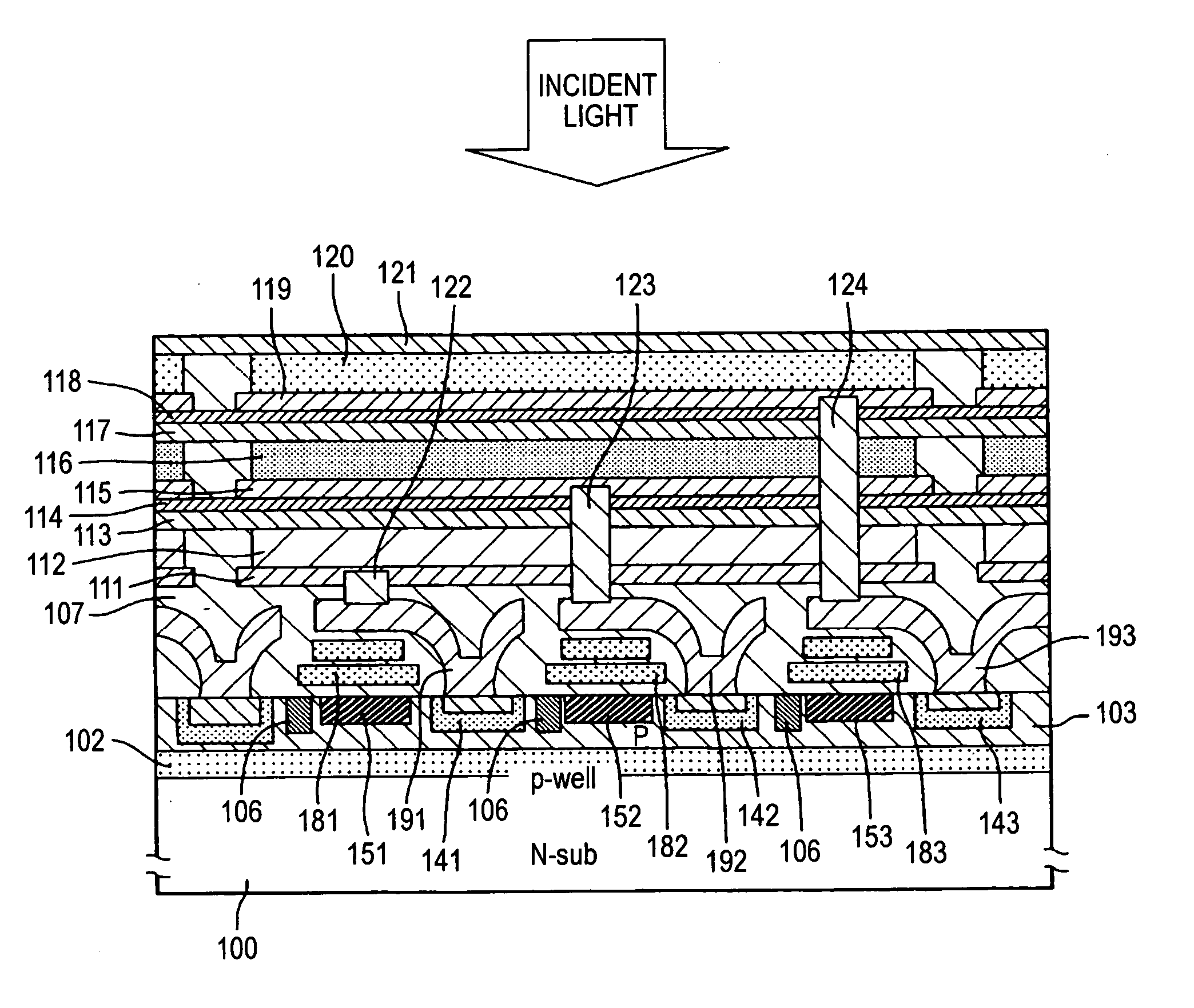
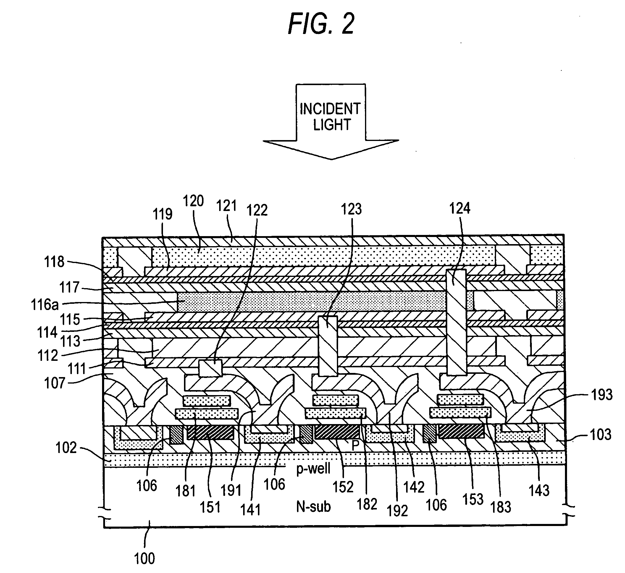
[0033]FIG. 1 is a typical sectional view corresponding to one pixel of a photoelectric converting layer lamination type solid-state image pick-up device according to the invention. A signal reading circuit is formed in a surface portion of a semiconductor substrate 100. The signal reading circuit may be constituted by an MOS transistor circuit in the same manner as in FIG. 5 or may be constituted by the same charge transfer path as that in the related-art CCD type image sensor as shown in FIG. 1.

[0034] In the photoelectric converting layer lamination type solid-state image pick-up device shown in FIG. 1, a P well layer 102 is formed in the surface portion of the n-type semiconductor substrate 100, and furthermore, a diode portion 141 to be a first color charge storage region, a diode portion 142 to be a second color charge storage region and a diode portion 143 to be a third color charge storage region are formed in a P region 103 in the surface portion and charge transfer paths 151...

third embodiment

[0051]FIG. 3 is a typical view showing a surface of a photoelectric converting layer lamination type solid-state image pick-up device according to the invention. In the photoelectric converting layer lamination type solid-state image pick-up device according to the embodiment, an area of a pixel 202 in a peripheral part of the device is set to be larger than that of a pixel 201 in a central part thereof. In other words, the area of the pixel is gradually increased from the central part of the device toward the peripheral part thereof.

[0052]FIG. 4A is a typical sectional view showing photoelectric converting layer portions of the pixel 201 in the central part of the device and the pixel 202 in the peripheral part of the device shown in FIG. 3. It is shown that areas of the photoelectric converting layers 112, 116 and 120 to be the first, second and third layers of the pixel 202 in the peripheral part of the device are larger than those of the photoelectric converting layers 112, 116 ...


PUM


Abstract

A photoelectric converting layer lamination type solid-state image pick-up device comprises: a semiconductor substrate; at least three layers of photoelectric converting layers each of which is interposed between a common electrode layer and pixel electrode layers, the pixel electrode layers corresponding to pixels respectively, wherein said at least three layers of photoelectric converting layers are laminated through insulating layers, said at least three layers of photoelectric converting layers being above the semiconductor substrate, and wherein each of said at least three layers of photoelectric converting layers is separated into layers corresponding the pixels respectively.

Description

BACKGROUND OF THE INVENTION [0001] 1. Field of the Invention [0002] The present invention relates to a solid-state image pick-up device in which a photoelectric converting layer for generating a signal charge corresponding to a quantity of an incident light is laminated on a semiconductor substrate on which a signal reading circuit is formed, and more particularly to a photoelectric converting layer lamination type solid-state image pick-up device in which S / N of an image signal obtained by a photoelectric converting layer is enhanced. [0003] 2. Description of the Related Art [0004] A prototype unit of a photoelectric converting layer lamination type solid-state image pick-up device has been described in JP-A-58-103165, for example. The solid-state image pick-up device has a structure that three photosensitive layers are laminated on a semiconductor substrate and respective electric signals for red (R), green (G) and blue (B) colors detected by each photosensitive layer are read by ...

Claims


Application Information

Patent Timeline
Patent Type & Authority Applications(United States)
IPC IPC(8): H01L27/00H01L27/146H04N5/369
CPCH01L27/14645
Inventor MIYASHITA, TAKESHIMISAWA, TAKESHI
Owner FUJIFILM CORP
Why Eureka
Try Eureka