Photoelectric conversion element and method for producing photoelectric conversion element

a technology of photoelectric conversion element and conversion element, which is applied in the direction of diodes, semiconductor devices, electrical apparatus, etc., can solve the problems of high transmittance and low resistance, high material and forming method restrictions, and achieve the effect of convenient fabrication reducing noise, and increasing the sensitivity of photoelectric conversion elements

Inactive Publication Date: 2006-08-31
FUJIFILM CORP +1
View PDF3 Cites 11 Cited by
  • Summary
  • Abstract
  • Description
  • Claims
  • Application Information

AI Technical Summary

Benefits of technology

[0010] According to the invention, it is possible to increase the sensitivity of a photoelectric conversion element and lower the noises thereof and, moreover, more conveniently fabricate the photoelectric conversion element.

Problems solved by technology

However, it has been a technical problem to establish both of a high transmittance and a low resistance in the formation of a transparent electrode.
To establish a low resistance, on the other hand, it is frequently observed that the material and forming method of the layer are highly restricted, for example, there arises the need for the crystallization of the layer material.

Method used


Image

  • Photoelectric conversion element and method for producing photoelectric conversion element
  • Photoelectric conversion element and method for producing photoelectric conversion element

Examples


example 1

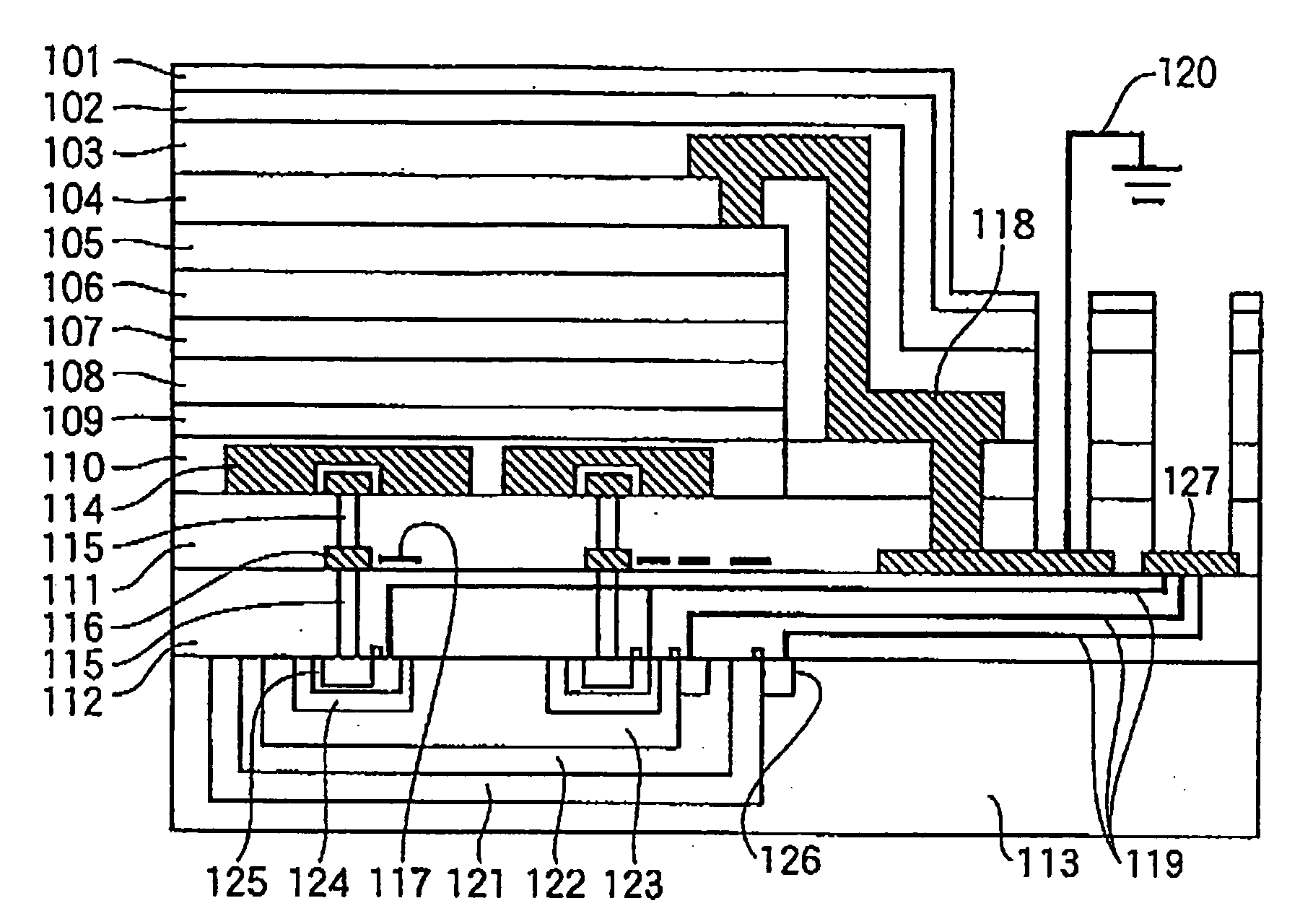
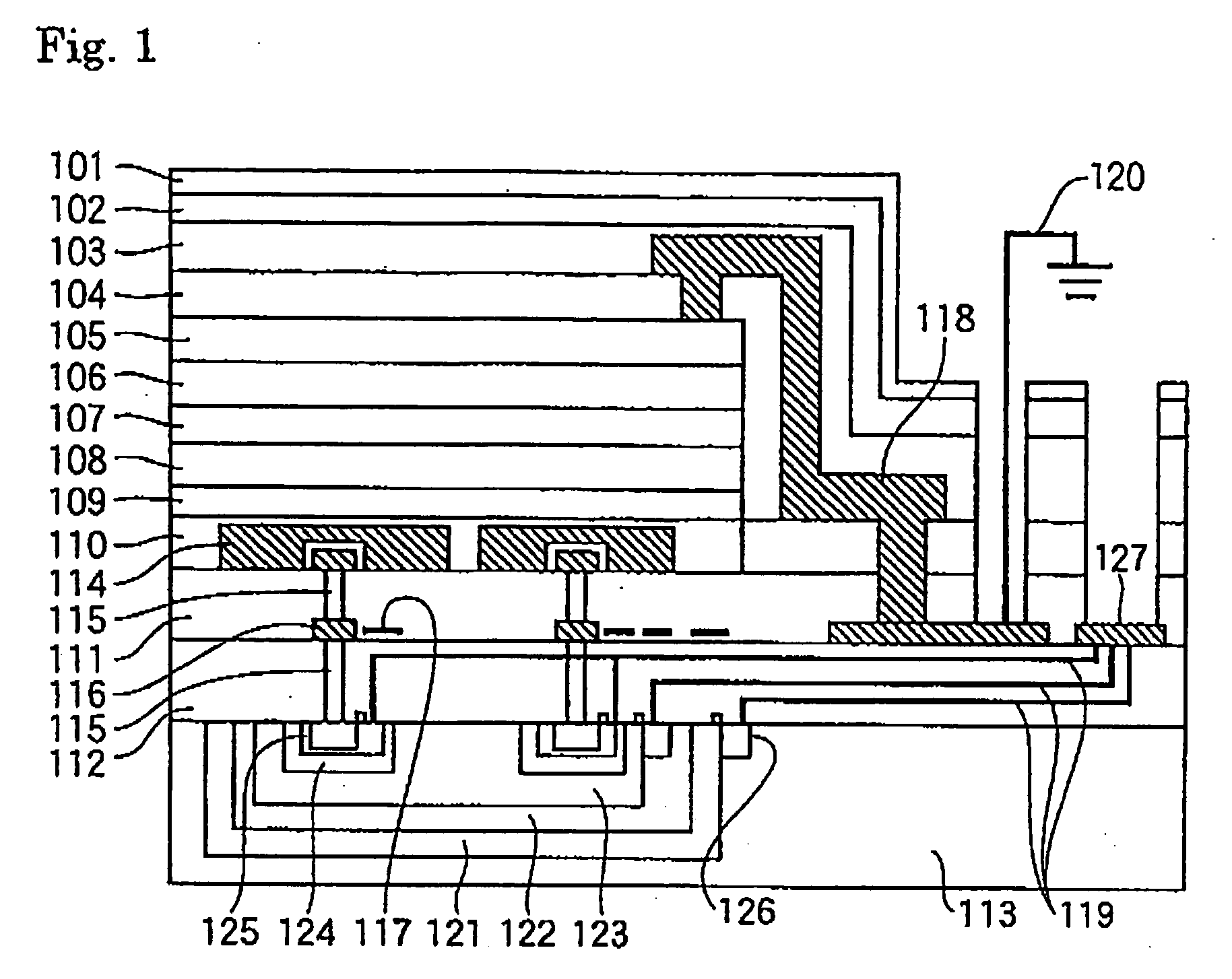
[0122] In the preferable photoelectric conversion element structure as discussed above, an MgAg layer of 10 nm in thickness was formed as a buffer layer 106. A pixel transparent electrode 114 was formed by using ITO and its layer thickness was 50 nm. The sheet resistance of the pixel transparent electrode 114 was 200Ω / □. In the case of the invention, a transparent electrode 105 was formed by the rf sputtering method (TS distance: 10 cm) wherein the O2 inlet amount corresponded to 4% of the total gas inlet amount and the layer-forming temperature was 25° C. In Comparative Example, on the other hand, a transparent electrode 105 was formed by introducing 0.5% of O2 based on the total gas inlet amount and the layer-forming temperature was 25° C. As substitutes for the organic layers 107 to 110 in the preferred photoelectric conversion element, a tris-8-hydroxyquinoline aluminum (Alq) layer (50 nm) and a 2,9-dimethylquinacridone layer were formed from the substrate side by the heat depos...

example 2

[0125] In the preferable photoelectric conversion element structure as described above, a transparent electrode 105 was formed by the rf sputtering method (TS distance: 10 cm) wherein the O2 inlet amount corresponded to 0% of the total gas inlet amount and the layer-forming temperature was 25° C. to give a layer 10 nm in thickness. In Comparative Example, on the other hand, a transparent electrode 105 was formed by introducing 0.5% of O2 and the layer-forming temperature was 25° C. to give a layer of 100 nm in thickness. As substitutes for the organic layers 106 to 110 in the preferred photoelectric conversion element, a tris-8-hydroxyquinoline aluminum (Alq) layer (50 nm) and a 2,9-dimethylquinacridone layer (100 nm) were formed from the substrate side by the heat deposition method.

[0126] As the results of the measurement of sheet resistances and transmittances of the transparent electrodes thus obtained, the sheet resistance of the invention sample was 1500Ω / □ while that of the c...


PUM


Abstract

A photoelectric conversion element comprising: a substrate; a conductive layer; a photoelectric conversion layer; and a transparent conductive layer, provided in this order, wherein the transparent conductive layer has a sheet resistance of from 100 to 10000Ω/□.

Description

FIELD OF THE INVENTION [0001] This invention relates to a photoelectric conversion element having a transparent electrode on a photoelectric conversion layer. BACKGROUND OF THE INVENTION [0002] In a photoelectric conversion element having a transparent electrode formed on a photoelectric conversion part, it has been regarded as favorable to achieve a higher transmittance of the transparent electrode and a lower resistance thereof so as to increase the absolute quantity of light falling into the photoelectric conversion part and increase the carrier reading efficiency after the photoelectric conversion, As the materials for forming the transparent electrode, transparent conductive oxide layer such as ITO is preferably used as a material having both of a high transmittance and a low resistance. However, it has been a technical problem to establish both of a high transmittance and a low resistance in the formation of a transparent electrode. In general, the resistance is liable to incr...

Claims


Application Information

Patent Timeline
Patent Type & Authority Applications(United States)
IPC IPC(8): H01L31/00
CPCH01L27/1462H01L27/14643H01L31/022408H01L31/1884Y02E10/50
Inventor MITSUI, TETSURO
Owner FUJIFILM CORP
Why Eureka
Try Eureka