Connection technology for power semiconductors comprising a layer of electrically insulating material that follows the surface contours

Inactive Publication Date: 2006-08-31
SIEMENS AG
View PDF8 Cites 9 Cited by
  • Summary
  • Abstract
  • Description
  • Claims
  • Application Information

AI Technical Summary

Benefits of technology

[0057] The described planar connection technology occupies a low overall height, resulting in a compact structure.
[0058] With multi-layer connecting planes, large-area metallization

Problems solved by technology

On the other, the layer of electrically insulating material next to the typically very tall performance component on the substrate is not

Method used


Image

  • Connection technology for power semiconductors comprising a layer of electrically insulating material that follows the surface contours
  • Connection technology for power semiconductors comprising a layer of electrically insulating material that follows the surface contours

Examples


Example

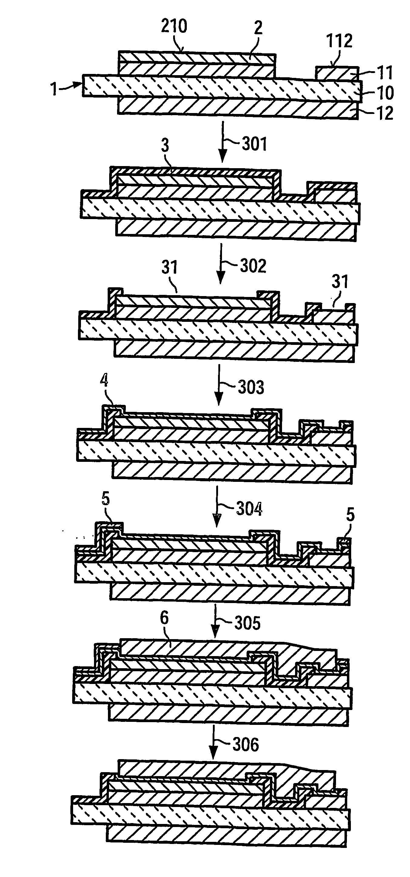
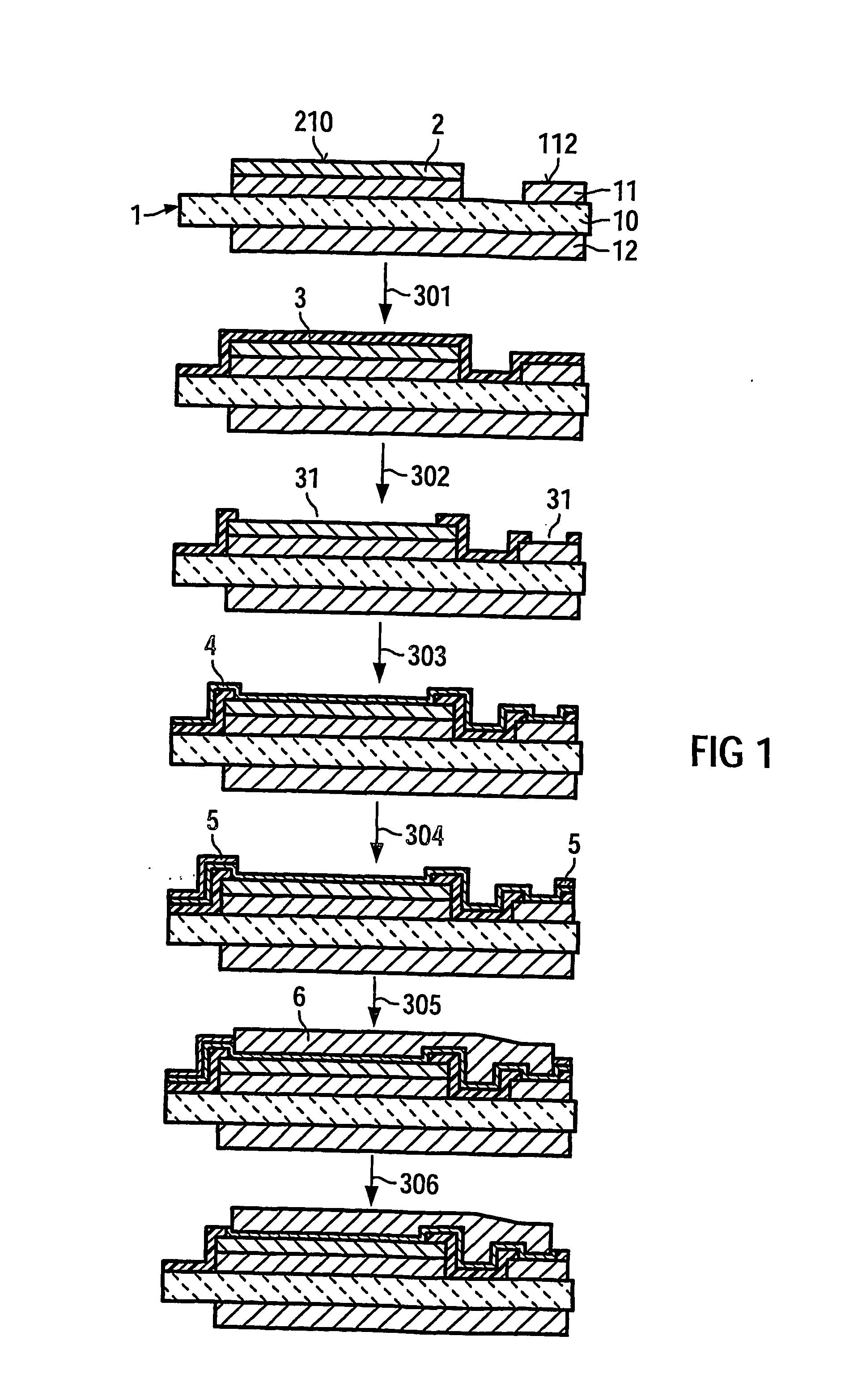
[0062] In FIG. 1, the substrate of the example is given the general label 1. This substrate 1 has a DCB substrate, for example, consisting of a substrate layer 10 of ceramic material, a copper layer 12 applied to a lower surface of the substrate layer 10, and a copper layer 11 applied to a surface of the substrate layer 10 facing away from the lower surface.

[0063] Areas of the layer 11 on the upper surface of the substrate layer 10 are removed down to the upper surface of the substrate 10, so that the upper surface is exposed there. The copper layers 11 and 12 form conductor tracks on the substrate.

[0064] One of more semiconductor chips 2, which may be identical to and / or different from each other, are applied to the surface of the remaining copper layer 11 facing away from the substrate layer 10.

[0065] The semiconductor chip 2, which is preferably a power semiconductor chip, makes planar contact with the upper surface of the layer 11 by a contact surface not shown, which exists ...


PUM


Abstract

A layer of electrically insulating material is applied to a substrate and a component located thereon, in such a way that said layer follows the surface contours.

Description

CROSS REFERENCE TO RELATED APPLICATIONS [0001] This application is the US National Stage of International Application No. PCT / EP2004 / 000629, filed Jan. 26, 2004 and claims the benefit thereof. The International Application claims the benefits of German application No. 10308978.0, filed Feb. 28, 2003. The International Application and the German application are incorporated by reference herein in their entirety:FIELD OF INVENTION [0002] The invention relates connection technology for power semiconductors comprising a layer of electrically insulating material that follows the surface contours. BACKGROUND OF THE INVENTION [0003] The most widely established technology for interconnecting power semiconductor chips and connecting them to conductor tracks is thick-wire bonding. Ultrasound energy is used to create a permanent connection between the Al wire, which has a typical diameter of several hundreds of μm, and the contact surface, which is of Al on the chip and Cu on the power module,...

Claims


Application Information

Patent Timeline
IPC IPC(8): H01L23/48H01L21/4763H01L21/60H01L23/538H01L25/07
CPCH01L23/5389H01L24/24H01L24/82H01L25/072H01L2224/2402H01L2224/24051H01L2224/24225H01L2224/24226H01L2924/01013H01L2924/0102H01L2924/01027H01L2924/01029H01L2924/01033H01L2924/01058H01L2924/01074H01L2924/01078H01L2924/01079H01L2924/01082H01L2924/01327H01L2924/09701H01L2924/19043H01L2924/30107H01L2924/3025H01L2924/01005H01L2924/01006H01L2924/014H01L2224/45147H01L2924/00H01L2224/45124H01L2924/00014H01L2224/48H01L2924/15787H01L2224/45015H01L2924/00011H01L2924/2076H01L2924/00015H01L2924/01004
Inventor SELIGER, NORBERTWEIDNER, KARLZAPF, JORG
Owner SIEMENS AG
Why Eureka
Try Eureka