Uniform single walled carbon nanotube network

a carbon nanotube and single-walled technology, applied in the field of carbon nanotubes, can solve problems such as non-uniform electrical properties of the nanotube network

Inactive Publication Date: 2006-08-31
MOTOROLA INC
View PDF2 Cites 22 Cited by
  • Summary
  • Abstract
  • Description
  • Claims
  • Application Information

AI Technical Summary

Problems solved by technology

However, results are poor due to the inconsistency in nanotube diameter and density.
Different nanotube diameters result in variable bandgaps of individual nanotubes leading to non-uniform electrical properties of the nanotube network.

Method used


Image

  • Uniform single walled carbon nanotube network
  • Uniform single walled carbon nanotube network
  • Uniform single walled carbon nanotube network

Examples


Embodiment Construction

[0015] The following detailed description of the invention is merely exemplary in nature and is not intended to limit the invention or the application and uses of the invention. Furthermore, there is no intention to be bound by any theory presented in the preceding background of the invention or the following detailed description of the invention.

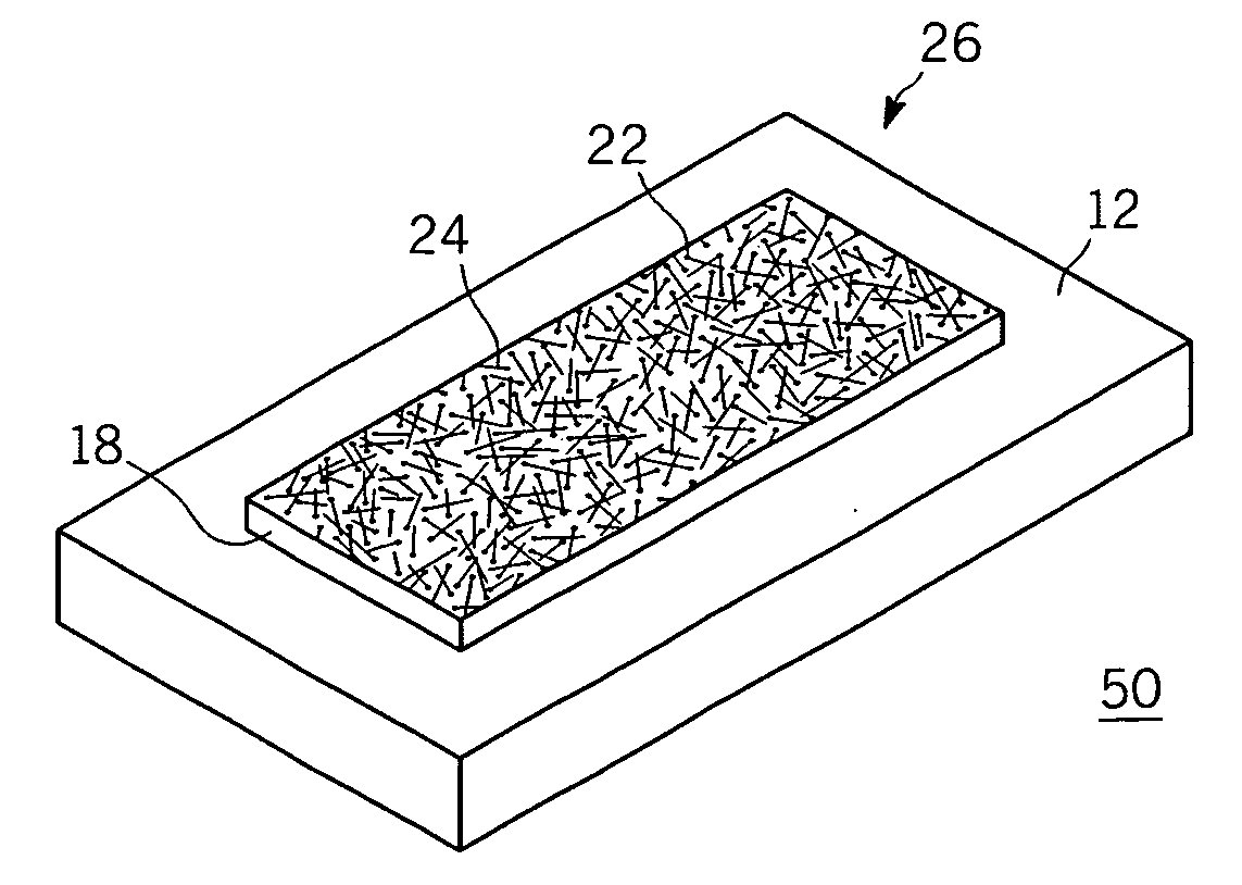
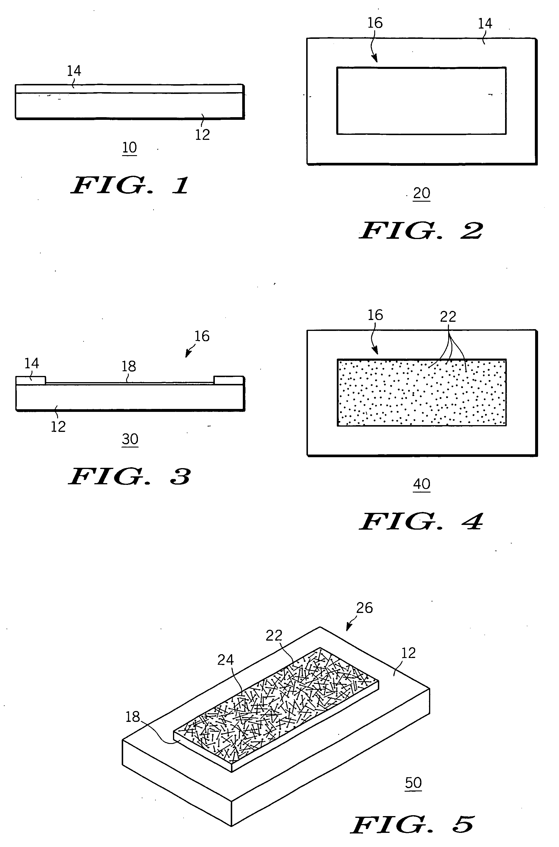
[0016] Referring to FIG. 1, a resist 14 is formed on a substrate 12 of the device 10. The substrate 12 preferably comprises silicon dioxide on silicon, but may alternatively comprise, for example, glass, ceramic or a flexible substrate. The resist would comprise any resist typically used in the semiconductor industry. Optionally, the layer 18 may be formed by a stamping technique known to those skilled in the industry without using the resist 14, as discussed below.

[0017] Referring to FIG. 2, some of the resist 14 is lifted, e.g., by a photo etch, to expose a portion 16 of the substrate 12. While only one portion 16 of the substrate 12 is...


PUM

PropertyMeasurementUnit
diameteraaaaaaaaaa
thicknessaaaaaaaaaa
diameteraaaaaaaaaa

Abstract

An apparatus (50) and method is provided for growing a network of common diameter nanotubes (24). The apparatus comprises chemically functionalizing a portion (16) of a substrate (12); anchoring catalyst nanoparticles (22), each having substantially the same diameter, on the portion (16) of the substrate (12); and growing overlapping carbon nanotubes (24), each having substantially the same diameter, on the catalyst nanoparticles (22).

Description

FIELD OF THE INVENTION [0001] The present invention generally relates to a carbon nanotubes and more particularly to a network of single walled carbon nanotubes. BACKGROUND OF THE INVENTION [0002] Carbon is one of the most important known elements and can be combined with oxygen, hydrogen, nitrogen and the like. Carbon has four known unique crystalline structures including diamond, graphite, fullerene and carbon nanotubes. In particular, carbon nanotubes refer to a helical tubular structure grown with a single wall or multi-wall, and commonly referred to as single-walled nanotubes (SWNTs), or multi-walled nanotubes (MWNTs), respectively. These types of structures are obtained by rolling a sheet formed of a plurality of hexagons. The sheet is formed by combining each carbon atom thereof with three neighboring carbon atoms to form a helical tube. Carbon nanotubes typically have a diameter in the order of a fraction of a nanometer to a few hundred nanometers. [0003] Carbon nanotubes ca...

Claims


Application Information

Patent Timeline
Patent Type & Authority Applications(United States)
IPC IPC(8): H01L31/0328B32B9/00B05D5/12B05D3/10
CPCB82Y10/00B82Y30/00B82Y40/00C01B31/0233Y10T428/30H01L51/0008H01L51/0048H01L51/0541C01B2202/36C01B32/162Y10T428/31663H10K71/16H10K85/221H10K10/464
Inventor AMLANI, ISLAMSHAH S.NAGAHARA, LARRY A.
Owner MOTOROLA INC
Why Eureka
Try Eureka