High density plasma chemical vapor deposition apparatus

a chemical vapor deposition and high density plasma technology, applied in chemical vapor deposition coatings, vacuum evaporation coatings, coatings, etc., can solve the problems of limited uniform deposition on the entire surface of the wafer, limited uniform deposition of cvd, and inability to meet the requirements of chemical vapor deposition

Inactive Publication Date: 2006-09-07
SAMSUNG ELECTRONICS CO LTD
View PDF4 Cites 359 Cited by
  • Summary
  • Abstract
  • Description
  • Claims
  • Application Information

AI Technical Summary

Benefits of technology

[0012] The present general inventive concept provides a high density plasma chemical vapor deposition apparatus, designed to provide uniform distribution of a

Problems solved by technology

When performing the CVD, it is necessary to perform a heat treatment for the wafer at a high temperature after deposition, which entails an unwanted side effect of semiconductor diode deterioration due to the high temperature.
Additionally, since semiconductor diodes are highly integrated, and a gap between metallic wires has become fine as a result of rapid development in semiconductor manufacturing technologies, the CVD has limitations in filling the gap between the metallic wires.
However, in the conventional gas distributing device, the upper gas supply nozzle for supplying the processing gases to the processing chamber has a single injection port formed in the vertical direction, so that the processing gases supplied through the upper gas supply nozzle are concentrated relatively on the center of the wafer,

Method used


Image

  • High density plasma chemical vapor deposition apparatus
  • High density plasma chemical vapor deposition apparatus
  • High density plasma chemical vapor deposition apparatus

Examples


Embodiment Construction

[0029] Reference will now be made in detail to the embodiments of the present general inventive concept, examples of which are illustrated in the accompanying drawings wherein like reference numerals refer to the like elements throughout the drawings. The embodiments are described below to explain the present general inventive concept while referring to the drawings.

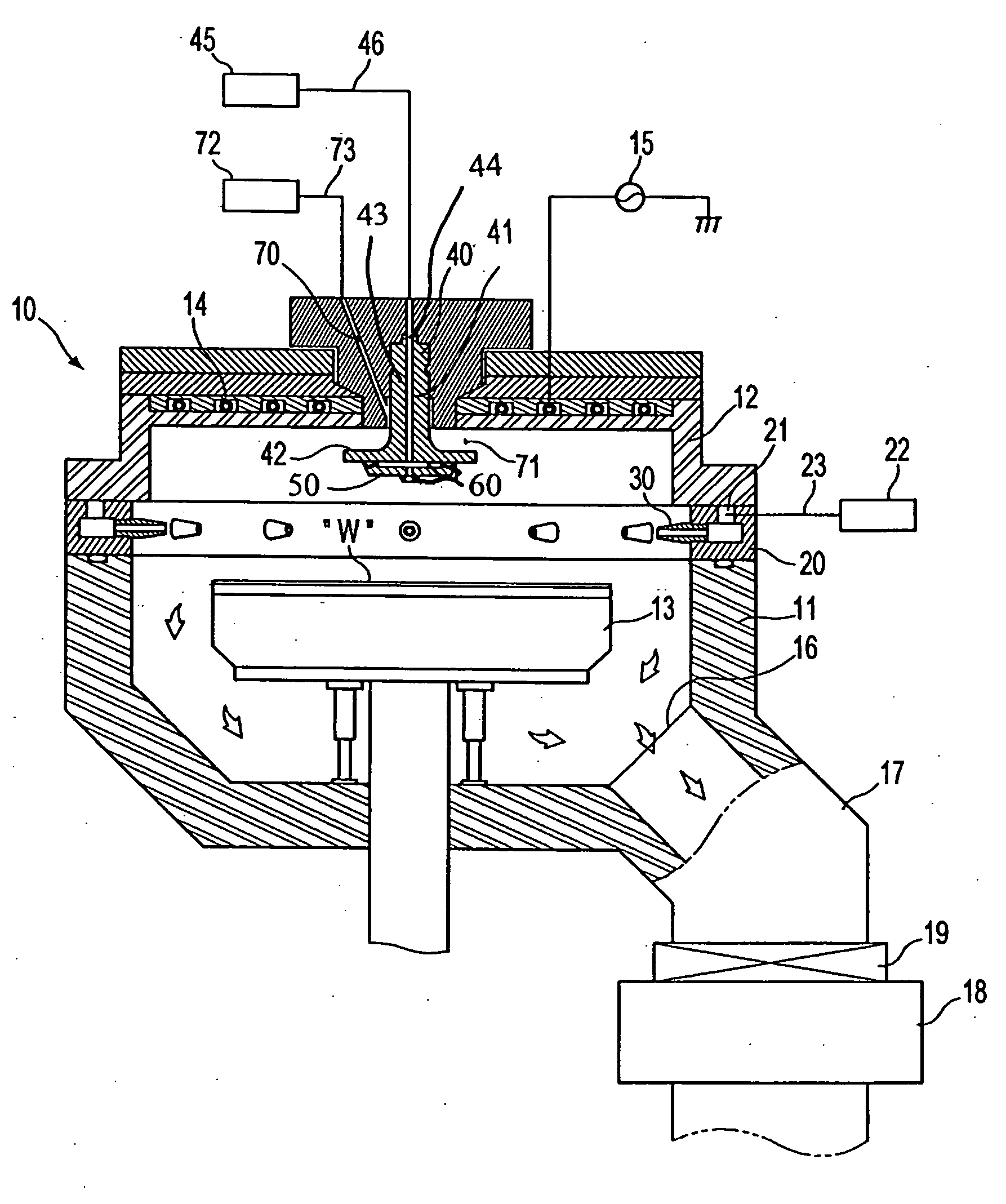
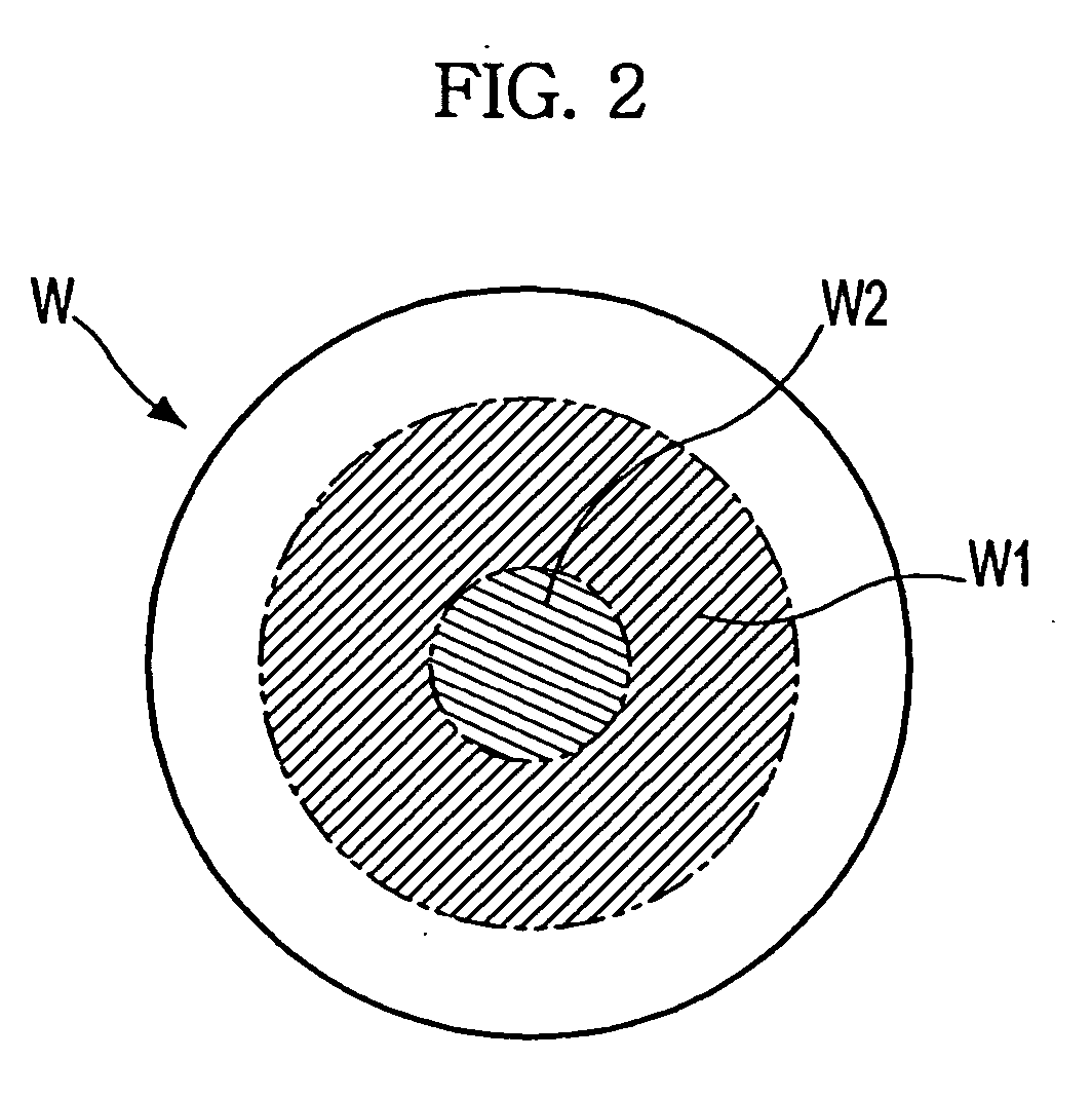
[0030]FIG. 1 is a cross-sectional view illustrating a high density plasma chemical vapor deposition apparatus according to the an embodiment of the present general inventive concept, and FIG. 2 is a schematic top view illustrating a semiconductor wafer W of FIG. 1. FIGS. 3 to 7 are cross-sectional views illustrating upper gas supply nozzles of the high density plasma chemical vapor deposition apparatus according to various embodiments of the present general inventive concept.

[0031] Referring to FIG. 1, a processing chamber 10 in which the semiconductor wafer W is processed includes a cylindrical chamber body 11 having ...


PUM

PropertyMeasurementUnit
Angleaaaaaaaaaa
Diameteraaaaaaaaaa
Densityaaaaaaaaaa

Abstract

A high density plasma chemical vapor deposition apparatus includes an upper gas supply nozzle which includes a nozzle body, a gas supply passage formed vertically in the nozzle body, a nozzle cover attached to a lower surface of the horizontal portion of the nozzle body, and a plurality of gas inlets formed through the nozzle cover to uniformly supply the processing gas towards a semiconductor wafer within the processing chamber.

Description

CROSS-REFERENCE TO RELATED APPLICATIONS [0001] This application claims the benefit of Korean Patent Application No. 2005-17420, filed on Mar. 2, 2005 in the Korean Intellectual Property Office, the disclosure of which is incorporated herein in its entirety by reference. BACKGROUND OF THE INVENTION [0002] 1. Field of the Invention [0003] The present general inventive concept relates to a high density plasma chemical vapor deposition apparatus, and more particularly, to a high density plasma chemical vapor deposition apparatus which has a gas supply nozzle enhanced in structure such that processing gas supplied to a semiconductor wafer is uniformly injected from the gas supply nozzle. [0004] 2. Description of the Related Art [0005] Chemical vapor deposition (CVD) is one form of semiconductor processing technology, and refers to a process for forming a semiconductor film or an insulating film of a single crystal on a surface of a wafer by use of a chemical reaction. When performing the...

Claims


Application Information

Patent Timeline
IPC IPC(8): C23C14/00C23C16/00
CPCC23C16/45563C23C16/45565C23C16/509H01J37/3244H01L21/205
Inventor USHAKOV, ANDREYCHOI, JIN HYUKPARK, JONG ROK
Owner SAMSUNG ELECTRONICS CO LTD
Why Eureka
Try Eureka