Method for precisely controlled masked anodization

a technology of masking and anodization, which is applied in the direction of coatings, surface reaction electrolytic coatings, electrolytic coatings, etc., can solve the problem of self-limitation of the anodization process, and achieve the effect of improving and cost-efficien

Inactive Publication Date: 2012-05-31
INTERUNIVERSITAIR MICRO ELECTRONICS CENT (IMEC VZW) +1
View PDF4 Cites 23 Cited by
  • Summary
  • Abstract
  • Description
  • Claims
  • Application Information

AI Technical Summary

Benefits of technology

[0012]It is an object to provide an improved method for creating precise patterns of anodized material within an anodizable layer by means of masked anodization. More specifically it is an object to create precise patterns of a dielectric or porous material within a conductive thin film using mas

Problems solved by technology

Since the electrical current needed for the anodization process is supplied at the edge (perimeter) of the substrate, surrounding every group of structures on the anodization mask with an additional surrounding mask structure (defini

Method used


Image

  • Method for precisely controlled masked anodization
  • Method for precisely controlled masked anodization
  • Method for precisely controlled masked anodization

Examples


examples

[0103]By way of illustration, preferred embodiments not being limited thereto, a number of further particular examples are discussed below, illustrating features and advantages of preferred embodiments.

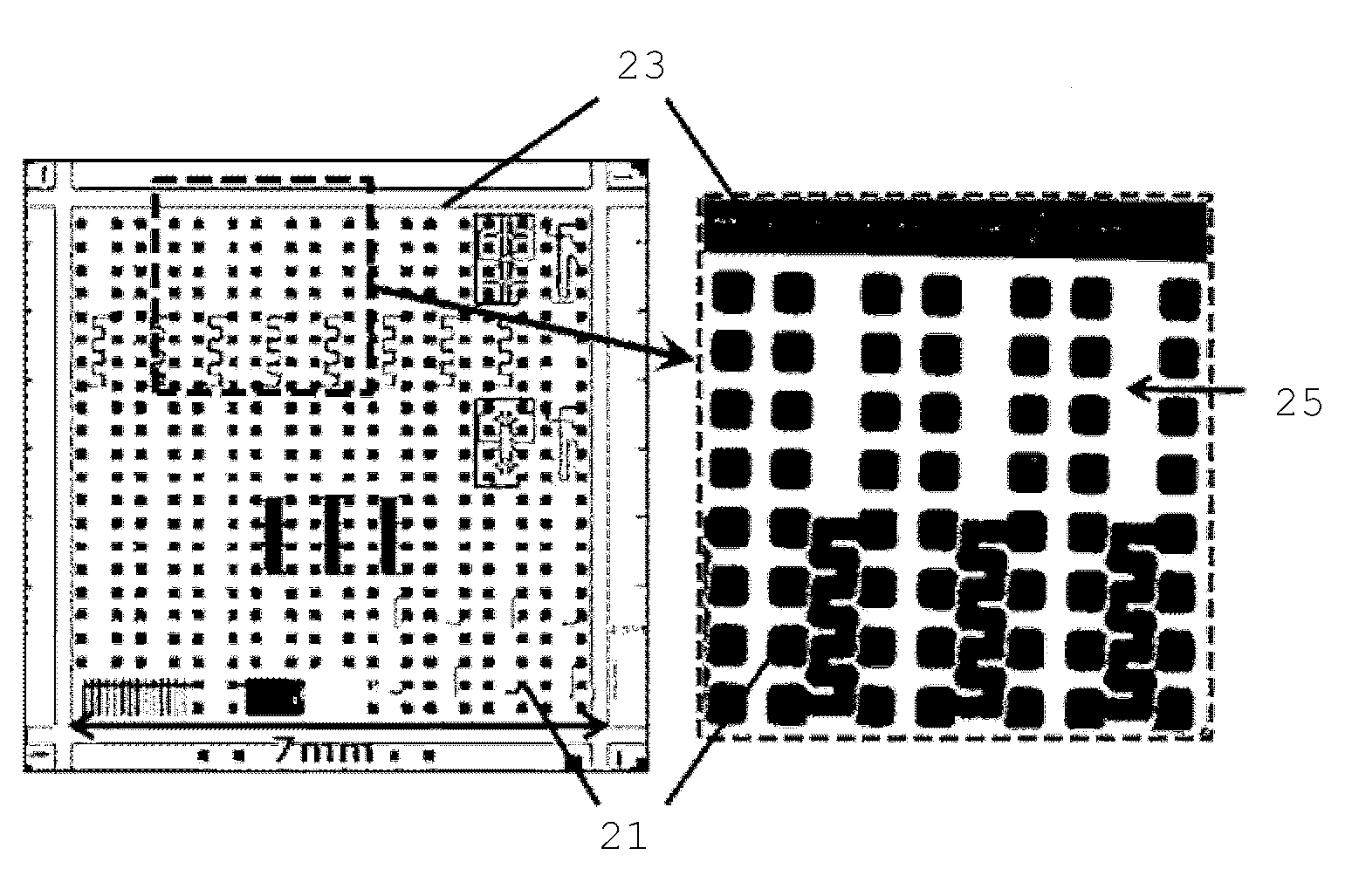
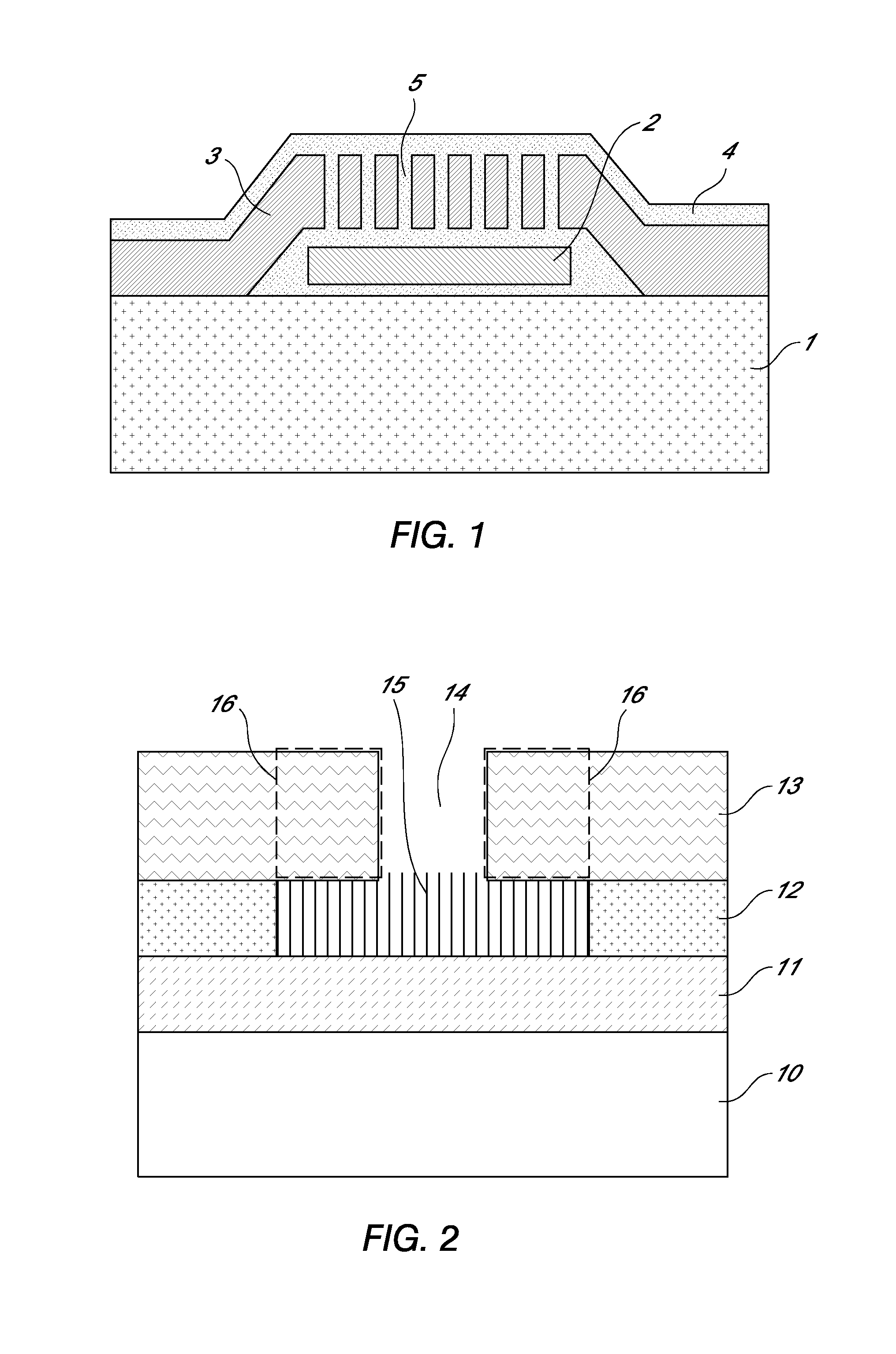
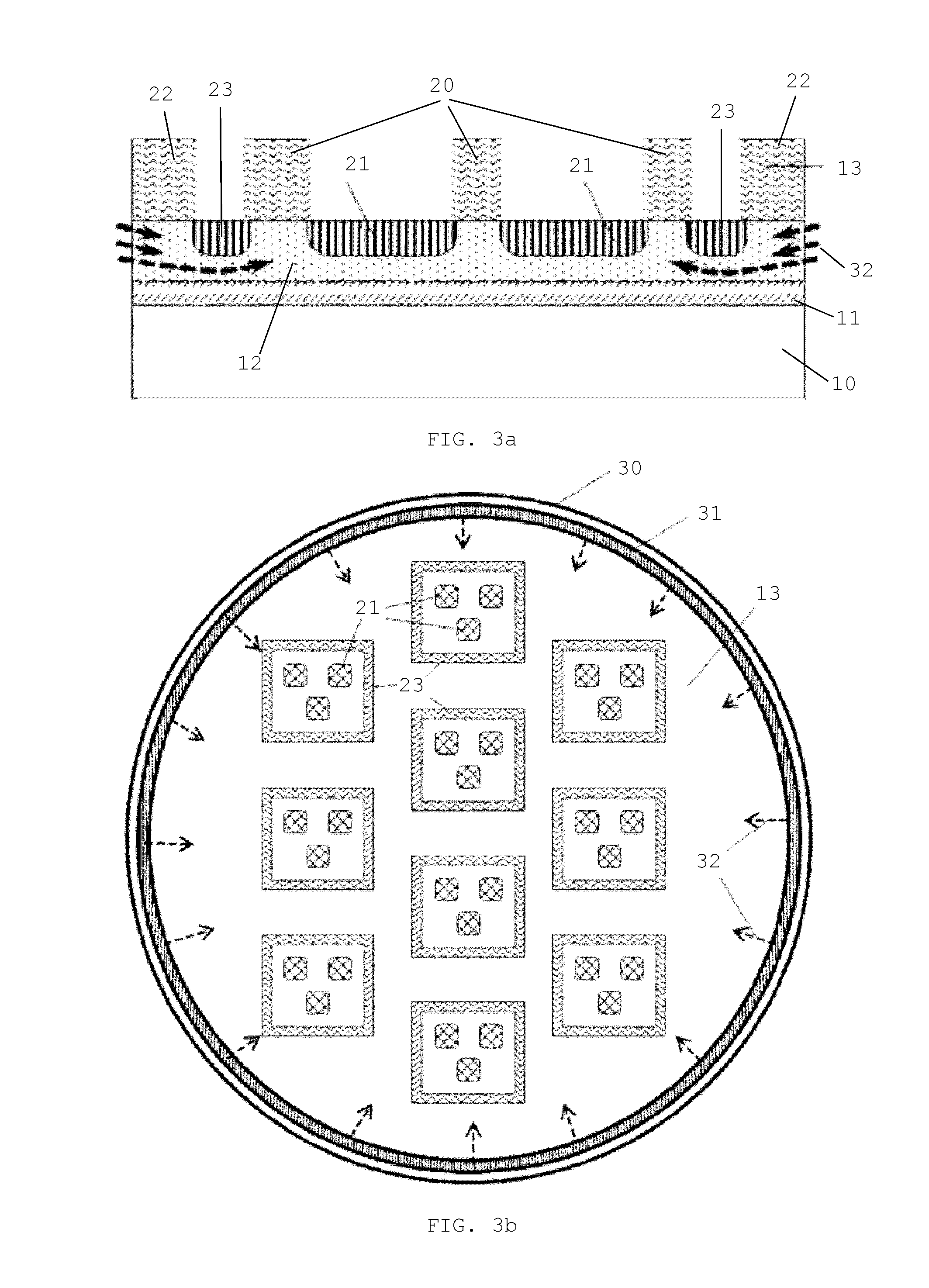
[0104]In a first particular example, anodization of a 1 μm-thick Al layer (deposited by sputtering on top of a silicon oxide layer on 200 mm Si wafer) has been performed using a photoresist mask not including the border line structure resulting in a large unwanted extension of the anodization region width from 160 μm up to 800 μm as shown in FIG. 2. The anodization process is performed in a Teflon-based chamber housing a sulfuric acid-based electrolyte. The anodization temperature and voltage used here are within the range of 20-30° C. and 10-20V respectively. By performing the same anodization process of an Al layer using a photoresist mask defining a border line 23 (ring) surrounding a plurality of other structures 21 as shown in FIG. 6, the anodization region width has been well co...


PUM

PropertyMeasurementUnit
Temperatureaaaaaaaaaa
Electric potential / voltageaaaaaaaaaa

Abstract

The present invention is related to a method for masked anodization of an anodizable layer on a substrate, for example an aluminum layer present on a sacrificial layer, wherein the sacrificial layer needs to be removed from a cavity comprising a Micro or Nano Electromechanical System (MEMS or NEMS). Anodization of an Al layer leads to the formation of elongate pores, through which the sacrificial layer can be removed. According to the method of the invention, the anodization of the Al layer is done with the help of a first mask which defines the area to be anodized, and a second mask which defines a second area to be anodized, said second area surrounding the first area. Anodization of the areas defined by the first and second mask leads to the formation of an anodized structure in the form of a closed ring around the first area, which forms a barrier against unwanted lateral anodization in the first area.

Description

CROSS-REFERENCE TO RELATED APPLICATION[0001]This application claims the benefit under 35 U.S.C. §119(e) of U.S. Provisional Application No. 61 / 418,194, filed Nov. 30, 2010, the disclosure of which is hereby expressly incorporated by reference in its entirety and is hereby expressly made a portion of this application.FIELD OF THE INVENTION[0002]Methods for precisely controlling a masked anodization process are provided. The preferred embodiments are further related to manufacturing semiconductor devices, especially to methods of encapsulation and to such devices. More specifically they may relate to zero-Level or wafer level packaging of semiconductor devices. More particularly, the preferred embodiments relate to Nano- and / or Micro-Electro-Mechanical Systems (NEMS and / or MEMS) and to processes of encapsulating (or packaging) said systems.BACKGROUND OF THE INVENTION[0003]Creating patterns of a dielectric or porous material within a conductive thin film by means of masked anodization ...

Claims


Application Information

Patent Timeline
IPC IPC(8): C25D11/02C25D11/18C25D5/02
CPCC25D11/12C25D11/18C25D11/246C25D11/022C25D11/10C25D11/24C25D11/08
Inventor ZEKRY, JOSEPHTILMANS, HENDRIKUSHOOF, CHRIS VANPUERS, ROBERT
Owner INTERUNIVERSITAIR MICRO ELECTRONICS CENT (IMEC VZW)
Why Eureka
Try Eureka