Method of manufacturing devices to protect election components

a manufacturing method and electronic circuit technology, applied in the direction of emergency protective arrangements for limiting excess voltage/current, coupling device connection, protective switch operation/release mechanism, etc., can solve the problem of increasing not completely eliminating the risk of damage attributed to such disturbances, and more modern devices operating in the higher frequencies (ghz and above) using submicron line widths are more susceptible to damage which cannot be overcome using such methods. , to achieve the effect o

Inactive Publication Date: 2006-01-03
ELECTRONICS POLYMERS NEWCO
View PDF15 Cites 74 Cited by
  • Summary
  • Abstract
  • Description
  • Claims
  • Application Information

AI Technical Summary

Benefits of technology

[0014]An advantage of the present invention is that protection devices can be manufactured in high volumes using well known printed circuit board (PCB) manufacturing techniques. With the present invention, a panel holding anywhere from several hundred up to many thousand protection devices can be achieved with a combination of mixing, coating, curing, lamination, photo etch, and electroding steps. As a result, application specific designs can be readily customized and changes made quickly with minimal effort and expense.
[0015]Another advantage is that added capacitance can be limited by controlling the size of the electrode, formulation fillers and overall thickness of the devices.
[0016]Another advantage of the present invention is the achievement of a low profile protection device compared to the known prior art. For example, according to one embodiment a device profile of 5 mils is achievable compared to known prior art protection components that occupy between 15 and 30 mils.
[0017]Still another advantage of the invention is significant cost reductions compared to the prior art due primarily to the elimination of a substrate and use of printed wafer board technologies to create panels containing as many as 100,000 devices measuring 0603 mils and smaller.
[0018]And still another advantage is the ability to control the capacitance of the protection device by altering the nature of the filler characteristics utilized in the polymer. Depending on the restrictions placed on added capacitance for a given application, a polymer formulation with more or less capacitance can be utilized. In addition, minimum overlap can also be used to reduce added capacitance.

Problems solved by technology

In general, such problems arise from the occurrence of electrical events that cause the transfer of charge from one material to another creating a surge in voltage due to voltage potential differences between the two materials.
While such techniques have been effectively used to shield a product from charge and to reduce the generation of charge caused by any movement of the product within the container housing the device to be protected, they have not completely eliminated the risk of damage attributed to such disturbances.
Moreover, it is well known that more modern devices operating in the higher frequencies (GHz and above) using submicron line widths are more susceptible to damage which cannot be overcome using such methods.
Such prior art protection components, however, suffer from several limitations attributed to the requirement that a substrate or reinforcing layer be used.
Specifically, the use of a substrate adds significantly to the component's overall size and cost.
In addition, the relatively large size and profile of such prior art protection components makes their use impractical in tight spaces where board space is limited.
Moreover, since the substrate material is a primary expense in the manufacture of such components, the use of prior art protection components on a widespread basis can be cost prohibitive.
In such an application, a prior art ESD protection component could not be cost effectively used on each pin and, in most situations, would occupy too much board space and be too thick to be practical.

Method used


Image

  • Method of manufacturing devices to protect election components
  • Method of manufacturing devices to protect election components
  • Method of manufacturing devices to protect election components

Examples


Embodiment Construction

[0029]The present invention provides a process of making a substrate-less protection device using standard printed circuit board (PCB) manufacturing techniques thereby allowing the manufacture of large number of devices relatively inexpensively. With the present invention, multiple ESD protection devices can be manufactured in panels that can be custom formed for an unlimited number of applications. It is believed that the process of the present invention has implications toward the manufacture of an all PCB protection system such as flex circuit with total ESD protection and / or as a layer in a PCB with protection provided for sensitive integrated circuits.

Manufacturing a Protection Device in Panels Gives Maximum Yield in High Quantities

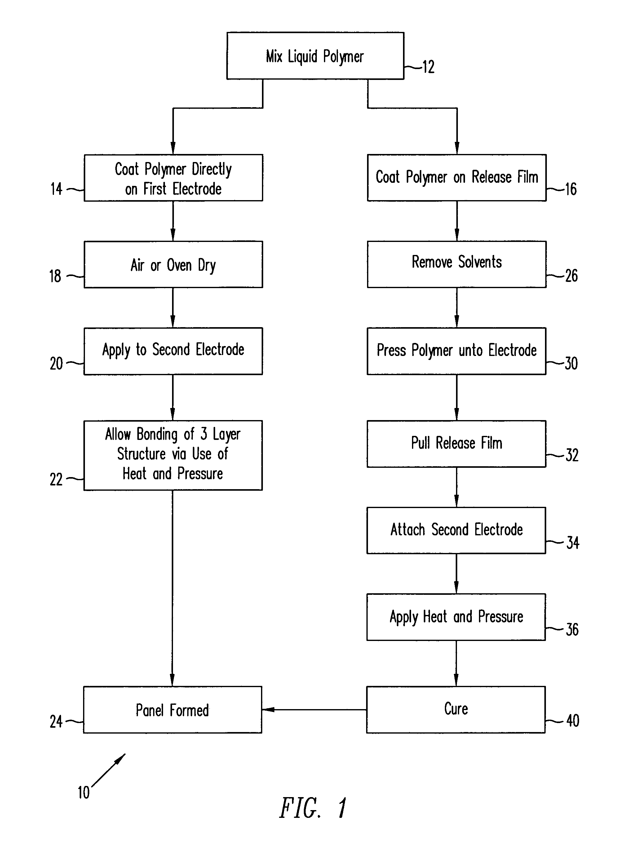
[0030]In general, the process of building a protection device according to the invention involves the use of a polymer-based formulation (or polymeric solution) that is coated directly on the electrodes forming the terminals of the protection device....


PUM

PropertyMeasurementUnit
pressureaaaaaaaaaa
insulatoraaaaaaaaaa
viscosityaaaaaaaaaa

Abstract

Devices capable of protecting electronic components during the occurrence of a disturbance event using printed circuit board manufacturing techniques. A three (3) layer structure is formed comprising a polymer-based formulation sandwiched between two electrode layers. The devices can be manufactured in panel form providing high quantities of devices which can be removed from the panel and applied directly to the component to be protected. Desired patterns can be formed on either one of the electrode layers by photo-etch techniques thereby providing a process that can be tailored to a large number of applications.

Description

TECHNICAL FIELD[0001]The present invention relates to electronic circuit protection devices and methods of making same. More particularly, the invention relates to the use of standard printed circuit board manufacturing processes for mass production of low profile polymer-based protection devices. Still more particularly, the invention relates to the manufacture of substrate-less protection devices that can be custom formed for use in a wide array of electronic circuit protection applications, such as electrostatic discharge and surge suppression, with possible implications toward the manufacture of a complete PCB protection system. Even still more particularly, the method of making such devices takes advantage of the vast know-how used in making printed circuit wiring boards and allows devices to be made in panels with features such as plated through-holes and multiple layers.BACKGROUND OF THE INVENTION[0002]The problems of static electricity and Electrostatic Discharge (ESD) are w...

Claims


Application Information

Patent Timeline
Patent Type & Authority Patents(United States)
IPC IPC(8): H05K3/02H01C7/00H01C17/065H01R13/648H05K1/02H05K1/03H05K1/16
CPCH01C7/005H01C17/06586H01R13/6485H05K1/0259H05K1/0373H05K1/167Y10T29/49222H05K2201/0738Y10T29/49195Y10T29/49146Y10T29/49156Y10T29/49155Y10T29/49107H05K3/0052
Inventor SHRIER, KAREN P.
Owner ELECTRONICS POLYMERS NEWCO
Why Eureka
Try Eureka