Semiconductor device, magnetic sensor, and magnetic sensor unit

a technology of magnetic sensor and magnetic sensor, which is applied in the direction of semiconductor/solid-state device details, galvano-magnetic devices, instruments, etc., can solve the problems of bending degrading the characteristics of the magnetosensitive portion, and fluctuating or degrading the characteristics of the sensor element 99, so as to prevent fluctuations and degradation of the characteristics, and reduce the size of the magnetic sensor

Active Publication Date: 2006-09-07
YAMAHA CORP
View PDF7 Cites 4 Cited by
  • Summary
  • Abstract
  • Description
  • Claims
  • Application Information

AI Technical Summary

Benefits of technology

[0023] By means of a semiconductor device of this invention, when mounting the semiconductor device on a mounting board as an external circuit, the semiconductor device is pressed against the mounting surface of the mounting board in a state in which the surface side of the semiconductor chip faces the mounting surface of the mounting board. Here, the sensor element and electrode portion are arranged in positions which do not overlap, and the stress at the electrode portion due to the pressing which reaches the sensor element can be reduced.
[0068] By means of the invention of the fourteen aspect, the heights from the rear surface of the circuit board to the top of each step are different, so that the magnetic sensor chips can easily be inclined with respect to the surface of the circuit board.

Problems solved by technology

That is, when a semiconductor device is mounted on a mounting board, or when a semiconductor device is caused to operate, the stress on the bump electrodes 97 and wiring layers reaches the sensor elements 99, and so there is the problem that the characteristics of the sensor elements 99 may fluctuate or be degraded.
However, in the case of the above magnetic sensor of the prior art, because the magnetosensing surface holding plate and the magnetosensitive portion are heated, when the magnetosensing surface holding plate and the magnetosensitive portion comprise materials with different thermal expansion coefficients, bending of the magnetosensitive portion occurs due to the difference in thermal expansion coefficients.
And when bending occurs in the magnetosensitive portion, there is the problem that the characteristics of the magnetosensitive portion are degraded, and the three-dimensional direction of an external magnetic field cannot be measured accurately.

Method used


Image

  • Semiconductor device, magnetic sensor, and magnetic sensor unit
  • Semiconductor device, magnetic sensor, and magnetic sensor unit
  • Semiconductor device, magnetic sensor, and magnetic sensor unit

Examples


Embodiment Construction

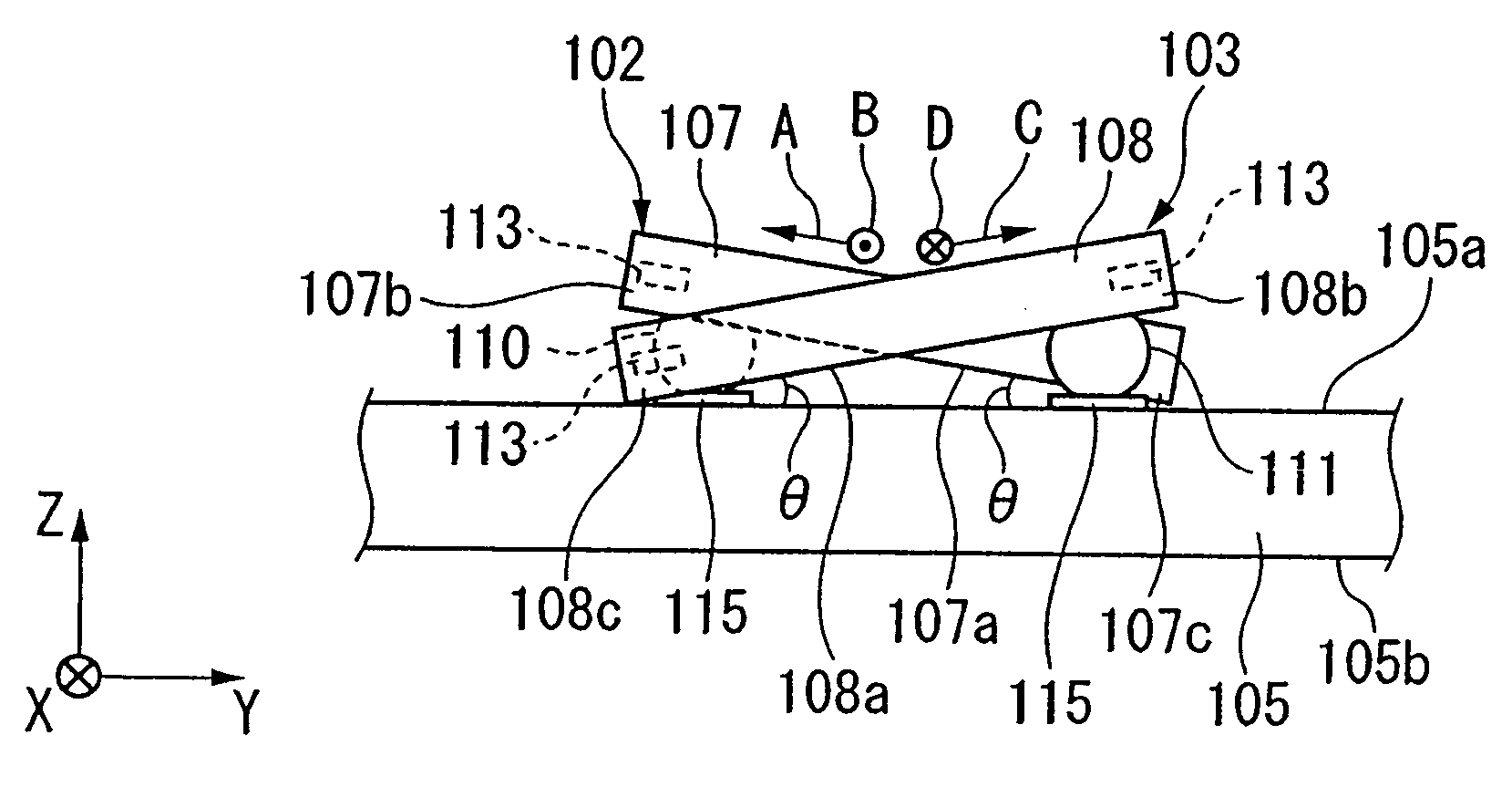
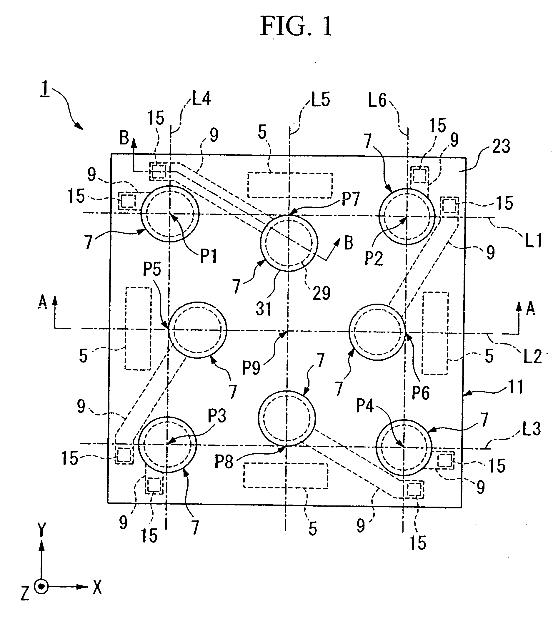
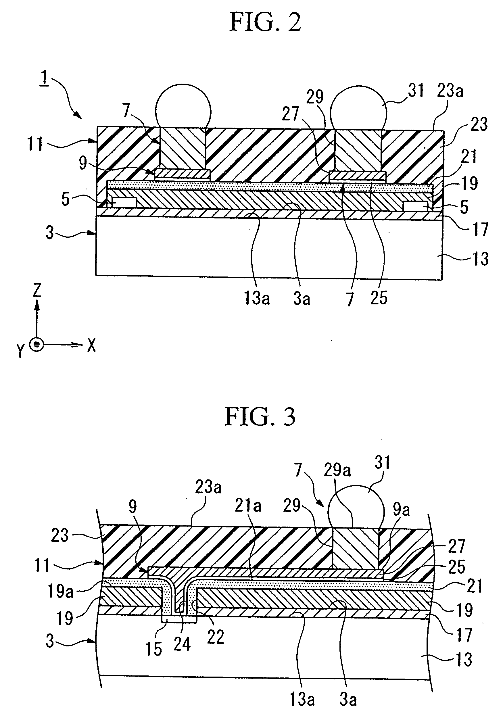
[0097]FIG. 1 to FIG. 3 show one aspect of the invention; the semiconductor device of this aspect is one type of wafer-level CSP (hereafter called a “WLCSP”), with electrodes for connection to the external circuitry of the mounting board provided at positions which do not protrude from the main face of the semiconductor chip on which the integrated circuits are formed. As shown in FIG. 1 and FIG. 2, this semiconductor device 1 comprises a semiconductor chip 3 in a sheet shape, formed into substantially a rectangular shape in plane view; a plurality of thin film magnetic elements 5, provided on the main face (surface) of the semiconductor chip 3; electrode portions 7, placed on the side of the main face 3a of the semiconductor chip 3, for connection of the semiconductor chip 3 to external circuitry; wiring portions 9 for electrical interconnection of the integrated circuits (not shown) of the semiconductor chip 3 and the electrode portions 7; and an insulating portion 11 which covers ...


PUM


Abstract

A semiconductor device, comprising a semiconductor chip; a pad electrode; an electrode portion; a wiring portion. An insulating portion is formed from electrically insulating material, covering the surface of the semiconductor chip and sealing the sensor element, wiring portion and electrode portion, in a state which exposes at least the electrode portion on the surface of the semiconductor chip. The electrode portion is placed in a position which does not overlap with the sensor element in the thickness direction of the semiconductor chip.

Description

BACKGROUND OF THE INVENTION [0001] 1. Field of the Invention [0002] This invention relates to a semiconductor device of the surface-mountable type, such as chip-size packages or similar. [0003] This invention further relates to a magnetic sensor and magnetic sensor unit for measurement of the direction of a magnetic field. [0004] Priority is claimed on Japanese Patent Applications No. 2004-87139, filed Mar. 24, 2004, and No. 2004-87140, filed Mar. 24, 2004, the content of which is incorporated herein by reference. [0005] 2. Description of the Related Art [0006] Recent years have seen the appearance of LSI and other semiconductor devices formed in dimensions substantially the same as those of the semiconductor chip, such as chip-size packages (hereafter called “CSPs”) and similar, and capable of surface mounting. Such technologies are attracting attention as mounting technologies suitable for smaller and lighter electronic equipment (see for example Japanese Patent Application, First...

Claims


Application Information

Patent Timeline
Patent Type & Authority Applications(United States)
IPC IPC(8): H01L43/00G01B7/00G01R33/00G01R33/02G01R33/07G01R33/09H01L21/44H01L23/31H01L23/485H01L23/50H01L23/58
CPCG01R33/02G01R33/07G01R33/09H01L23/3114H01L2224/1134H01L2224/1308H01L2224/131H01L2924/01022H01L2924/01029H01L2924/01033H01L2924/01078H01L2924/01079H01L2924/14H01L2924/15311H01L2924/014H01L2924/00013H01L2924/01005H01L2924/01006H01L2924/01024H01L2924/01047H01L2224/13099H01L2224/16145H01L24/13H01L24/14H01L24/16H01L24/81H01L2224/1403H01L2224/14051H01L2924/15151H01L2924/181H01L2224/05024H01L2224/05008H01L2224/05026H01L2224/05001H01L2224/05147H01L2224/05166H01L2224/05171H01L2224/05647H01L2924/15159H01L2924/15153H01L24/05H01L24/06H01L2924/0001H01L2224/0615H01L2224/0603H01L2224/02377H01L24/02H01L2924/00H01L2924/00014H01L2224/02H01L23/50
Inventor NAITO, HIROSHISATO, HIDEKI
Owner YAMAHA CORP
Why Eureka
Try Eureka