Semiconductor device and method of stacking semiconductor chips

Inactive Publication Date: 2006-09-07
SHARP KK
View PDF19 Cites 39 Cited by
  • Summary
  • Abstract
  • Description
  • Claims
  • Application Information

AI Technical Summary

Benefits of technology

[0033] With the arrangement, the electrical contact pads on the first semiconductor chip are placed at such positions that form a mirror image of the electrical contact pads on the second semiconductor chip. That is, a common signal is supplied to interconnected electrical contact pads. Thus, the first semiconductor chip and the second semiconductor chip can share wiring connecting them to the substrate, and therefore requires fewer wires.
[0034] With the arrangement, the first semiconductor chip

Problems solved by technology

By contrast, stacking a semiconductor chip on another semiconductor chip of the same type or shape (external dimensions) which is already stacked may damage the wire bonding formed between the latter and the substrate, since the former possibly overlaps those wire bonding.
These semiconductor devices have various problems.
Spacers thinner than 200-micron or so do not meet this requirement and present an obstacle in trimming down the package (semiconductor device) in thickness.
This presents difficulty in reducing the semiconductor chip stack and resultant packaging in their thickness.
This presents difficulty in reducing the package (semiconductor device) in horizontal dimensions.
Manufacturing costs increase for these reasons.
The stepped part loses its mechanical strength, and the second semiconductor chip 52 may possibly develop cracks or otherwise break.
It is therefore difficult to stack semiconductor chips and form a package with reduced thickness and horizontal dimensions for the same reasons as with the spa

Method used


Image

  • Semiconductor device and method of stacking semiconductor chips
  • Semiconductor device and method of stacking semiconductor chips
  • Semiconductor device and method of stacking semiconductor chips

Examples


embodiment 1

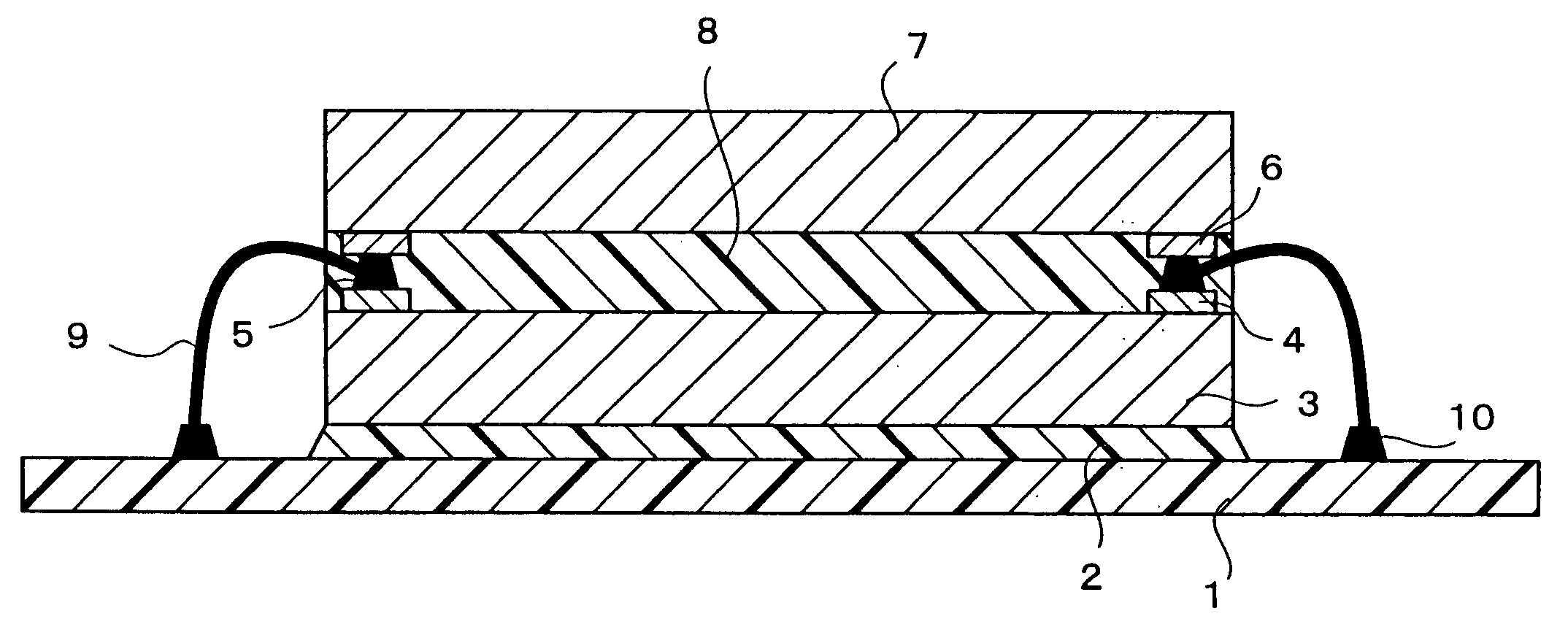
[0054] The following will describe an embodiment of the present invention in reference to FIGS. 1-3.

[0055] The semiconductor device of the present embodiment is a semiconductor device in which two or more semiconductor chips are stacked. Electrical contact pads are provided to both a first semiconductor chip and a second semiconductor chip at such positions that they form a mirror image on the first and second semiconductor chips, so those on the first semiconductor chip are located opposite to those on the second semiconductor chip when the first and second semiconductor chips are placed opposite to each other.

[0056] The method of stacking semiconductor chip of the present embodiment includes the steps of: placing the first and second semiconductor chips so that they are opposite to each other, the first and second semiconductor chips having electrical contact pads at such positions that they form a mirror image on the first and second semiconductor chips; and coupling the electr...

embodiment 2

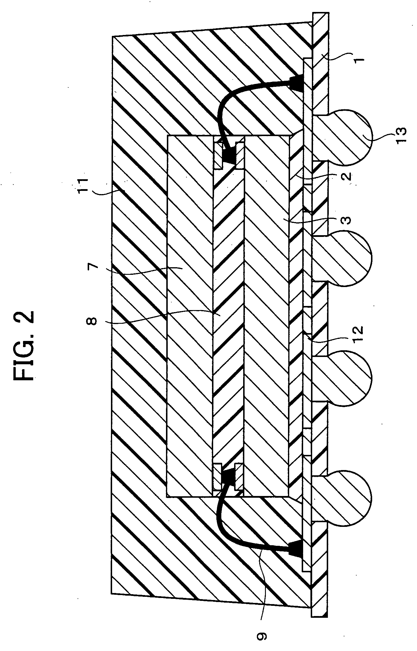
[0097] Referring to FIGS. 4, 5, the following will describe another embodiment of the present invention. Here, for convenience, members of the present embodiment that have the same arrangement and function as members (arrangement) shown in figures of embodiment 1, and that are mentioned in that embodiment are indicated by the same reference numerals and description thereof is omitted.

[0098] In the semiconductor device of the present embodiment, as shown in FIGS. 4, 5, a third chip (third semiconductor chip) 16 is stacked on a second chip 7 with an adhesion layer 15 interposed between them and has thereon third pads 17 which are electrically connected to the substrate 1. The third chip 16 has third pads (electrical contact pads) 17 on which are there formed bumps 18. The third pads 17 are connected by wires 19 to wire bonding terminals 20 on patterned wiring (not shown) on the substrate 1.

[0099] The third chip16 may be of the same type as or of a different type from the first chip ...

embodiment 3

[0106] Referring to FIGS. 6, 7, the following will describe another embodiment of the present invention. Here, for convenience, members of the present embodiment that have the same arrangement and function as members (arrangement) shown in figures of embodiments 1, 2 and that are mentioned in that embodiment are indicated by the same reference numerals and description thereof is omitted.

[0107] In the semiconductor device of the present embodiment, as shown in FIG. 6 and FIG. 7, a fourth chip (fourth semiconductor chip) 22 is stacked on a third chip 16 like mirror images. The third pads 17 on the third chip 16 form a mirror image of and connected to fourth pads 21 on the fourth chip 22 via bumps 18. Hence, an identical signal is supplied to the third pad 17 and the fourth pad 21 connected thereto. An interlayer adhesion layer 23 is formed between the third chip 16 and the fourth chip 22. The semiconductor device of the present embodiment is otherwise arranged in the same manner as (...


PUM


Abstract

In a semiconductor device, two or more semiconductor chips are stacked, a first semiconductor chip has electrical contact pads at such positions that form a mirror image of electrical contact pads provided on a second semiconductor chip; and the electrical contact pads on the first semiconductor chip are positioned opposite to and connected to the corresponding electrical contact pads on the second semiconductor chip. Thus, semiconductor chips can be stacked stably. The semiconductor device is reduced in thickness, and a method of stacking semiconductor chips is offered.

Description

FIELD OF THE INVENTION [0001] The present invention relates generally to a semiconductor device and particularly to such a semiconductor device that multiple semiconductor chips are stacked in a single package and also to a method of stacking semiconductor chips. BACKGROUND OF THE INVENTION [0002] Recent mobile phones and other mobile terminals have a capability to download information, such as email and games, over a network, and accordingly require additional functions and capacity in, for example, installed memory. Typically, multiple semiconductor chips are stacked in a single package to achieve larger memory capacity. [0003] Various methods are available to stack semiconductor chips. A popular example is wire bonding whereby semiconductor chips to be stacked are electrically connected to a substrate by means of wires. In the manufacture of packages using wire bonding technology, attention should be paid to avoid damaging wire bonding already formed between the substrate and the...

Claims


Application Information

Patent Timeline
IPC IPC(8): H01L23/48H01L23/12H01L21/60H01L25/065H01L25/07H01L25/18H01L29/06
CPCH01L25/0657H01L29/0657H01L2224/1134H01L2224/13144H01L2224/16145H01L2224/32225H01L2224/48091H01L2224/48471H01L2224/48479H01L2224/73265H01L2224/85051H01L2224/85986H01L2224/92247H01L2225/0651H01L2225/06513H01L2225/06555H01L2225/06575H01L2225/06586H01L2924/01079H01L2924/10158H01L2924/15311H01L2224/85186H01L2924/00014H01L2224/32145H01L2224/48227H01L2924/00012H01L2224/26145H01L2924/10155H01L2224/83139H01L2224/73204H01L2224/16225H01L2924/00H01L24/73H01L2224/05573H01L2224/05599H01L2224/4554
Inventor MIYATA, KOJIFUKUI, YASUKI
Owner SHARP KK
Why Eureka
Try Eureka