Self dc-bias high frequency logic gate, high frequency NAND gate and high frequency nor gate

a logic gate and high frequency technology, applied in the field of high frequency logic gates, can solve the problems of dc-bias consumption, dc-bias consumption is a significant source of power consumption, and the logic gate cannot be normally operated in the rf (radio frequency) band, so as to achieve the effect of not wasting electric power

Inactive Publication Date: 2006-09-07
SUNPLUS TECH CO LTD
View PDF6 Cites 205 Cited by
  • Summary
  • Abstract
  • Description
  • Claims
  • Application Information

AI Technical Summary

Benefits of technology

[0020] The present invention uses the impedance matching network configuration to provide a self DC-bias, such that the present invention can be operated in the RF band with very weak signals. In addition, the high f

Problems solved by technology

Therefore, the conventional logic gate cannot be normally operated in the RF (Radio Frequency) band when the signals are very weak (e.g. 0.9-1.1 V).
In addition, a constant current is required for normal operation, thus there is DC-bias consumption even when the logic gate is idle

Method used


Image

  • Self dc-bias high frequency logic gate, high frequency NAND gate and high frequency nor gate
  • Self dc-bias high frequency logic gate, high frequency NAND gate and high frequency nor gate
  • Self dc-bias high frequency logic gate, high frequency NAND gate and high frequency nor gate

Examples


Embodiment Construction

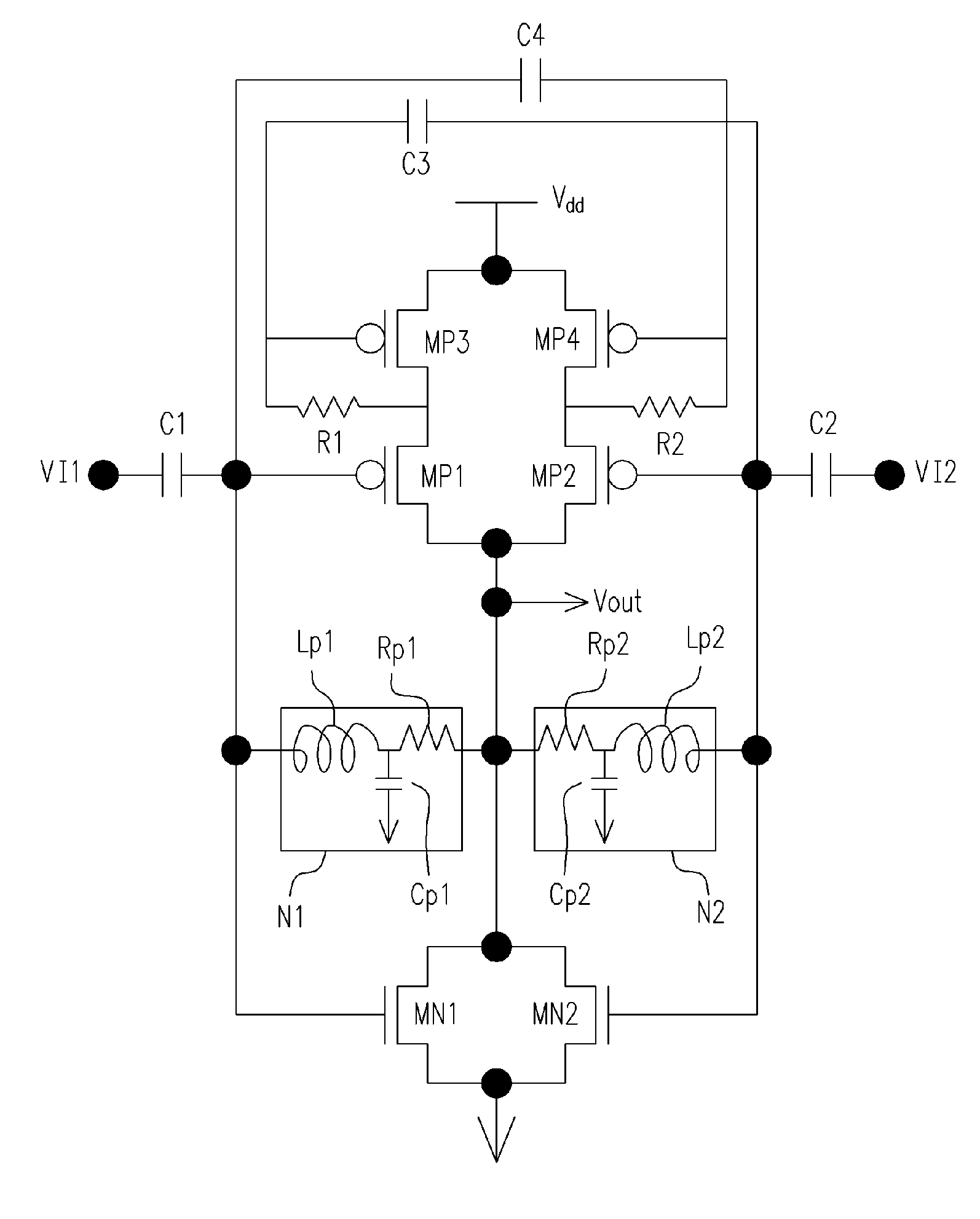
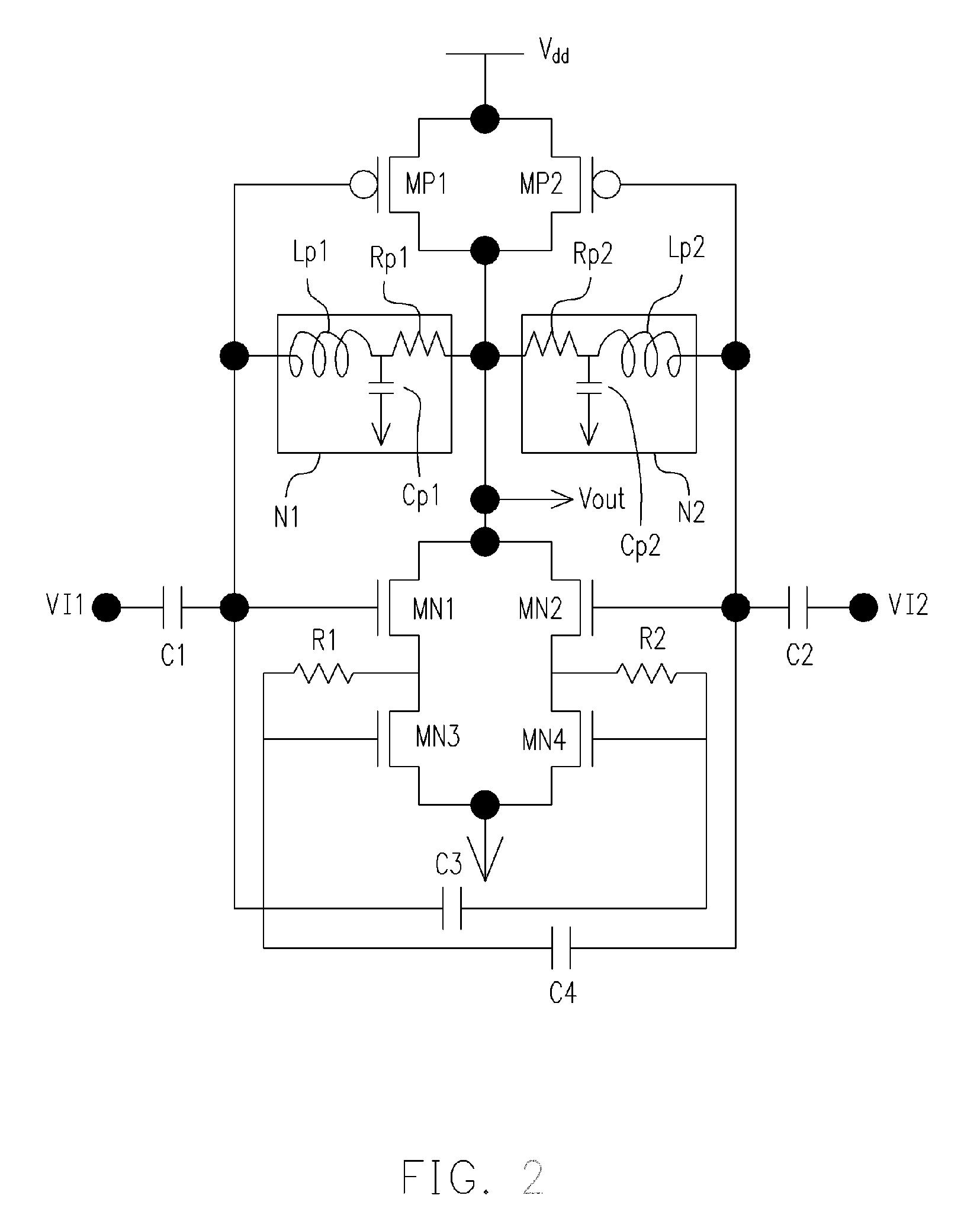
[0028]FIG. 2 schematically shows a high frequency NAND gate according to a preferred embodiment of the present invention using in the RF band with very weak signals. Referring to FIG. 2, the NAND gate comprises a first input terminal V11, a second input terminal V12, and an output terminal Vout for performing an NAND Boolean operation on the high frequency input signals and generating an operation result. The NAND gate further comprises the N type MOSFETs MN1, MN2, MN3, and MN4, the P type MOSFETs MP1 and MP2, the capacitors C1, C2, C3, and C4, the resistors R1 and R2, and the impedance matching networks N1 and N2. Wherein, the impedance matching network N1 comprises a matching inductance element Lp1, a matching capacitance element Cp1 and a matching resistance element Rp1. The first terminal of the matching inductance element Lp1 is the first terminal of the impedance matching network N1. The first terminal of the matching capacitance element Cp1 is electrically coupled to the seco...


PUM


Abstract

A self DC-bias high frequency logic gate is disclosed. The logic gate comprises at least one input terminal and one output terminal for performing Boolean operation on the high frequency input signals. The logic gate is characterized in that each transistor is coupled to an impedance matching network. The impedance matching network comprises a first terminal and a second terminal. Wherein, the first terminal is coupled to a gate of the transistor, and the second terminal is coupled to a drain of the transistor for providing an operation voltage to the transistor. When a gate of an N-type transistor and a gate of a P-type transistor are coupled with each other, and a drain of the N-type transistor and a drain of the P-type transistor are also coupled with each other, a common impedance matching network is shared with both the N-type transistor and the P-type transistor.

Description

CROSS-REFERENCE TO RELATED APPLICATION [0001] This application claims the priority benefit of Taiwan application serial no. 94106744, filed on Mar. 7, 2005. All disclosure of the Taiwan application is incorporated herein by reference. BACKGROUND OF THE INVENTION [0002] 1. Field of the Invention [0003] The present invention relates to a configuration of a digital logic gate, and more particularly, to a high frequency logic gate. [0004] 2. Description of the Related Art [0005] Along with continuous progress of electronic technique, it is the trend that digital system designs are to be faster, thinner and lighter. However, in order to have the logic gate operated normally, a higher input signal has to be fed into the conventional logic gate. Therefore, the conventional logic gate cannot be normally operated in the RF (Radio Frequency) band when the signals are very weak (e.g. 0.9-1.1 V). [0006] A logic gate using in the RF band had been proposed in the field. FIG. 1 schematically shows...

Claims


Application Information

Patent Timeline
IPC IPC(8): H03K19/20
CPCH03K19/0948
Inventor CHUNG, YUAN-HUNG
Owner SUNPLUS TECH CO LTD
Why Eureka
Try Eureka