Resistor integration structure and technique for noise elimination

a resistor and integrated circuit technology, applied in resistors, semiconductor devices, electrical equipment, etc., can solve the problems of oxidation of nicr and process that is somewhat uncontrolled, and achieve the effect of preventing contact noise, low noise, and low nois

Active Publication Date: 2006-09-07
TEXAS INSTR INC
View PDF2 Cites 4 Cited by
  • Summary
  • Abstract
  • Description
  • Claims
  • Application Information

AI Technical Summary

Benefits of technology

[0016] In one embodiment, the invention provides a low noise SiCr thin film resistor including an SiCr layer and a TiW layer disposed on a contact area of the SiCr layer without any discontinuous oxide between the SiCr layer and the TiW layer sufficient to cause noise-producing current-path-shifting of current flowing through both the SiCr layer and the TiW layer.
[0017] In another embodiment, the invention provides a low noise SiCr thin film resistor made by the method of preventing contact noise by performing in situ depositions of a SiCr layer and then a TiW layer on a substrate without breaking a vacuum between the depositions, to prevent formation of any discontinuous oxide between the SiCr layer and the TiW layer, patterning the SiCr and TiW layers to form a predetermined SiCr thin film resistor pattern and a TiW resistor contact pattern on the SiCr thin film resistor, and depositing and patterning a metallization layer to contact the TiW forming the resistor contact pattern.

Problems solved by technology

Generally, deposited NiCr oxidizes, and the process is somewhat uncontrolled because the oxidation of the NiCr causes its sheet resistance to shift as much as 20% or more during subsequent processing steps.

Method used


Image

  • Resistor integration structure and technique for noise elimination
  • Resistor integration structure and technique for noise elimination
  • Resistor integration structure and technique for noise elimination

Examples


Embodiment Construction

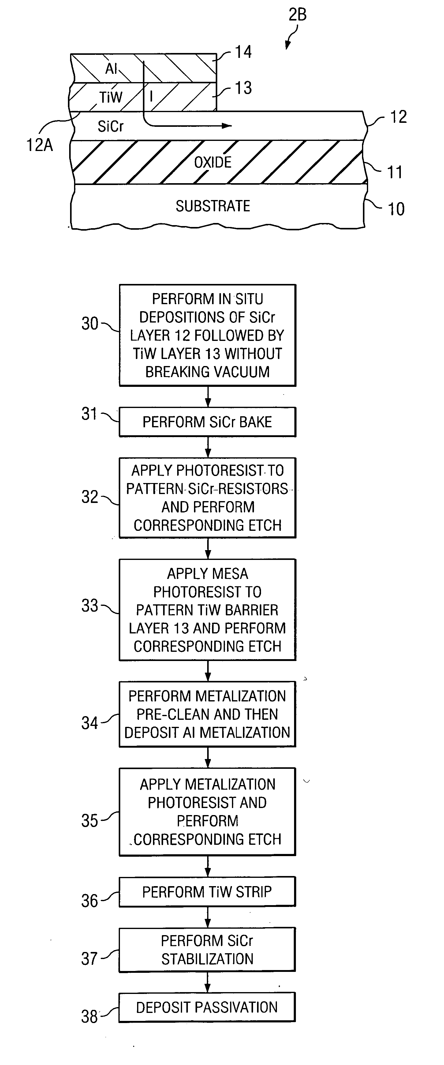
[0025] The present invention provides a way to provide low cost manufacture of low-noise SiCr thin film resistors in integrated circuits.

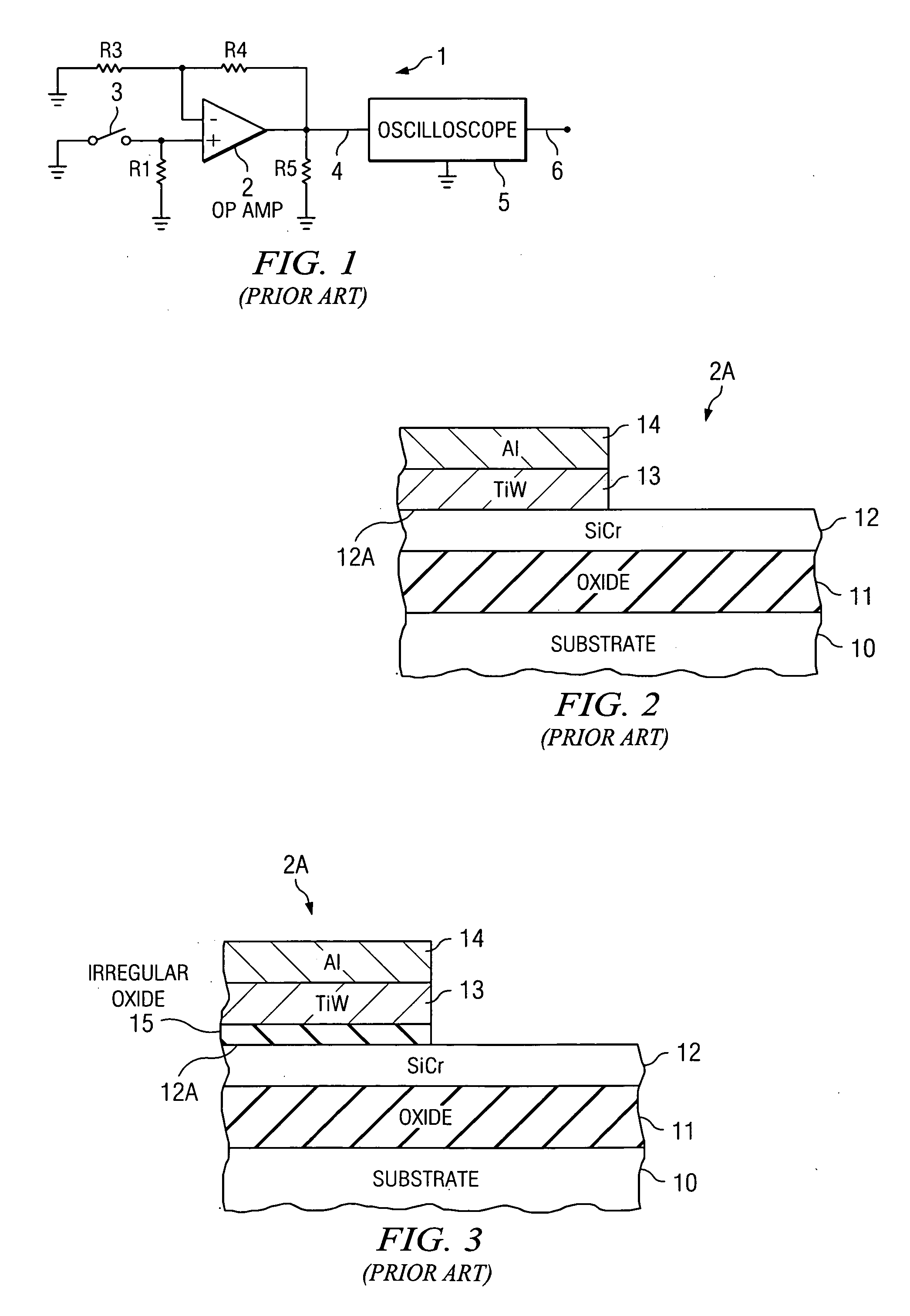
[0026] It was concluded that the above mentioned high noise levels (50.3 Pico amperes peak-to-peak) for operational amplifier 2 (FIG. 1) fabricated with standard SiCr thin film resistors was probably not due to the conventionally manufactured transistors in the operational amplifier 2. It was therefore concluded that the high measured noise was most likely due to the SiCr thin-film resistors. The most probable cause of the higher noise was thought to be due to a contact resistance problem at the interface between the SiCr and TiW layers.

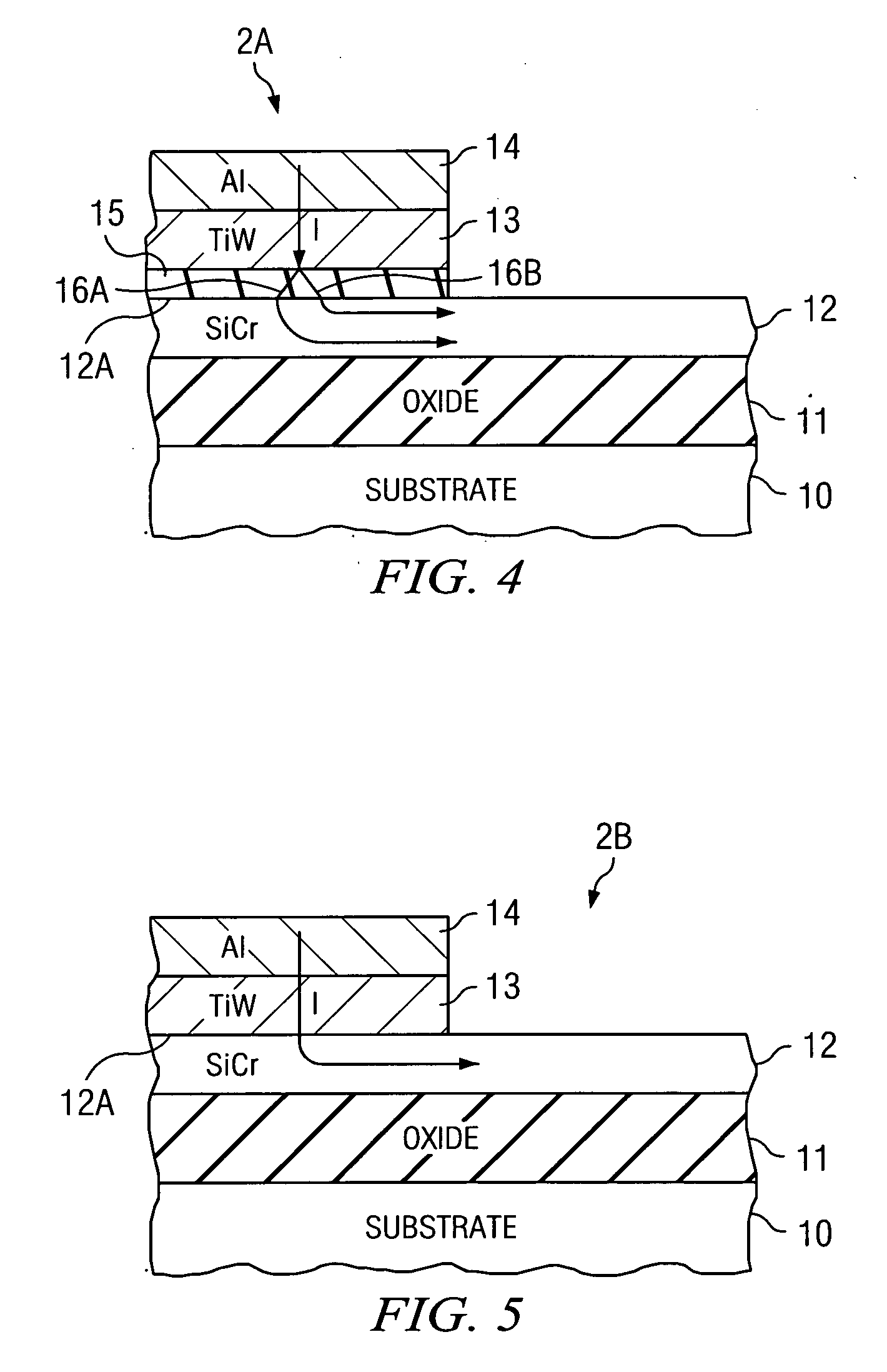
[0027]FIG. 3 shows a patterned aluminum layer 14 on a TiW barrier layer 13 formed over the contact area 12A of one end of a SiCr resistor 12 formed on a thick dielectric oxide 12 on integrated circuit substrate. A thin “hypothetical” irregular oxide layer 15 is believed to be present on the contact area 12A of one...


PUM


Abstract

A method of preventing contact noise in a SiCr thin film resistor includes performing in situ depositions of a SiCr layer and then a TiW layer on a substrate without breaking a vacuum between the depositions, to prevent formation of any discontinuous oxide between the SiCr layer and the TiW layer. The SiCr and TiW layers are patterned to form a predetermined SiCr thin film resistor pattern and a TiW resistor contact pattern on the SiCr thin film resistor, and a metallization layer is provided to contact the TiW forming the resistor contact pattern.

Description

BACKGROUND OF THE INVENTION [0001] The present invention relates generally to a new technique for providing inexpensive, low-noise integrated circuits, and more particularly to an improved technique for providing low noise SiCr thin film integrated circuit resistors without increasing integrated circuit processing costs. [0002]FIG. 1 illustrates a conventional noise testing circuit arrangement 1 for measuring the amount of noise produced by a circuit, which in this case is low-noise integrated circuit operational amplifier 2 including thin film resistors. The (−) input of operational amplifier 2 is connected between the junction between a gain resistor R3 and a feedback resistor R4. The (+) input is coupled to ground by a switch 3 and a resistor R1. The output of operational amplifier 2 is connected to an oscilloscope 5 which is used to determine the noise signal on the output of operational amplifier 2. [0003] SiCr (sichrome) thin film integrated circuit resistors are well known to...

Claims


Application Information

Patent Timeline
Patent Type & Authority Applications(United States)
IPC IPC(8): H01L21/84H01L21/00
CPCH01C7/006H01C7/18H01L28/24
Inventor JAISWAL, RAJNEESHBARBER, H. JEROMEKUEHL, THOMAS E.
Owner TEXAS INSTR INC
Why Eureka
Try Eureka