Semiconductor device and method of manufacturing the same

a technology of semiconductor devices and semiconductor electrodes, applied in semiconductor devices, semiconductor/solid-state device details, electrical apparatus, etc., can solve the problems of insufficient protection of the underlying gate electrodes, difficult formation of small contact holes by conventional methods,

Inactive Publication Date: 2006-09-14
SAMSUNG ELECTRONICS CO LTD
View PDF13 Cites 11 Cited by
  • Summary
  • Abstract
  • Description
  • Claims
  • Application Information

AI Technical Summary

Benefits of technology

[0021] It is a first feature of the present invention to provide a semiconductor device which can prevent an electrical short-circuit between a lower wiring and an upper wiring.
[0022] It is a second feature of the present invention to provide a method of manufacturing a semiconductor device for preventing an electrical short-circuit between a lower wiring and an upper wiring.
[0023] It is a third feature of the present invention to provide a method of manufacturing a DRAM device which can prevent an electrical short-circuit between a storage node contact and a gate electrode or between a bit line contact and the gate electrode.

Problems solved by technology

As a result, the formation of small contact holes by conventional methods becomes very difficult.
Hence, the gate mask layers 20 do not sufficiently protect the underlying gate electrodes 18.

Method used


Image

  • Semiconductor device and method of manufacturing the same
  • Semiconductor device and method of manufacturing the same
  • Semiconductor device and method of manufacturing the same

Examples


Embodiment Construction

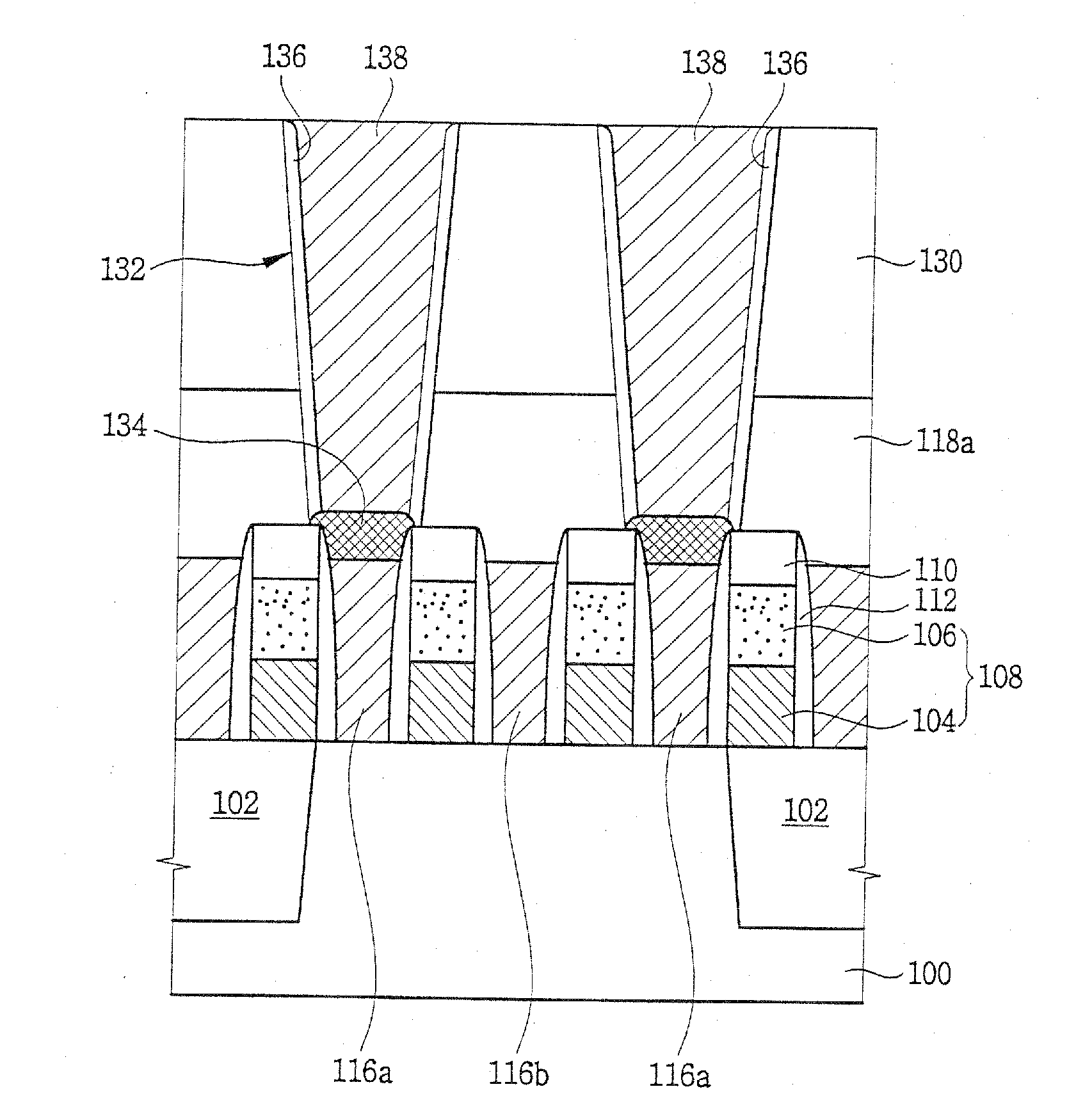
[0028] The invention now will be described more fully hereinafter with reference to the accompanying drawings, in which preferred embodiments of the invention are shown. This invention may, however, be embodied in many different forms and should not be construed as limited to the embodiments set forth herein; rather, these embodiments are provided so that this disclosure will be thorough and complete, and will fully convey the scope of the invention to those skilled in the art. Like numbers refer to like elements throughout. The relative thickness of layers in the illustrations may be exaggerated for purposes of describing the invention.

[0029]FIGS. 2A to 2E are cross-sectional diagrams illustrating a method of manufacturing a semiconductor device according to an embodiment of the invention.

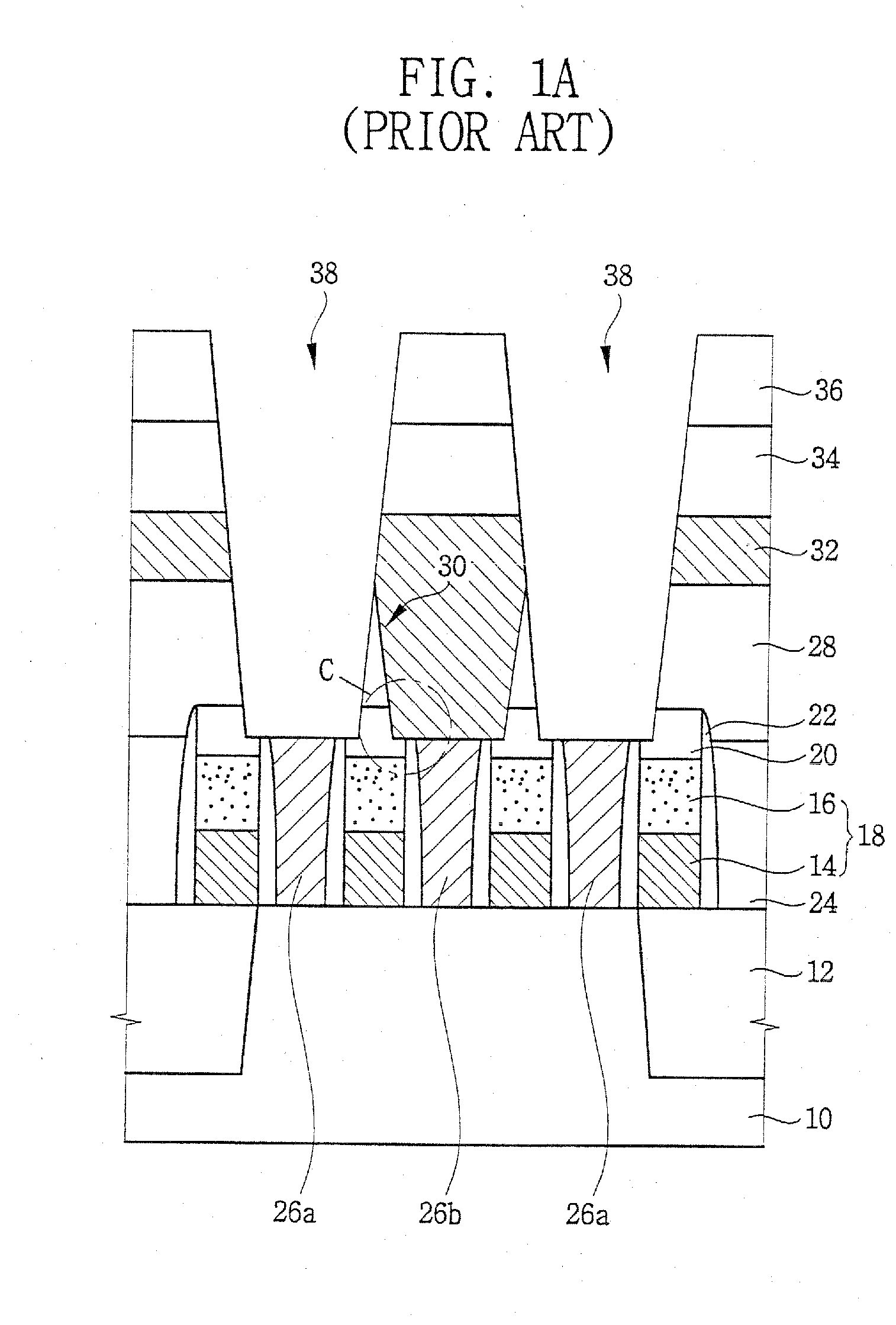
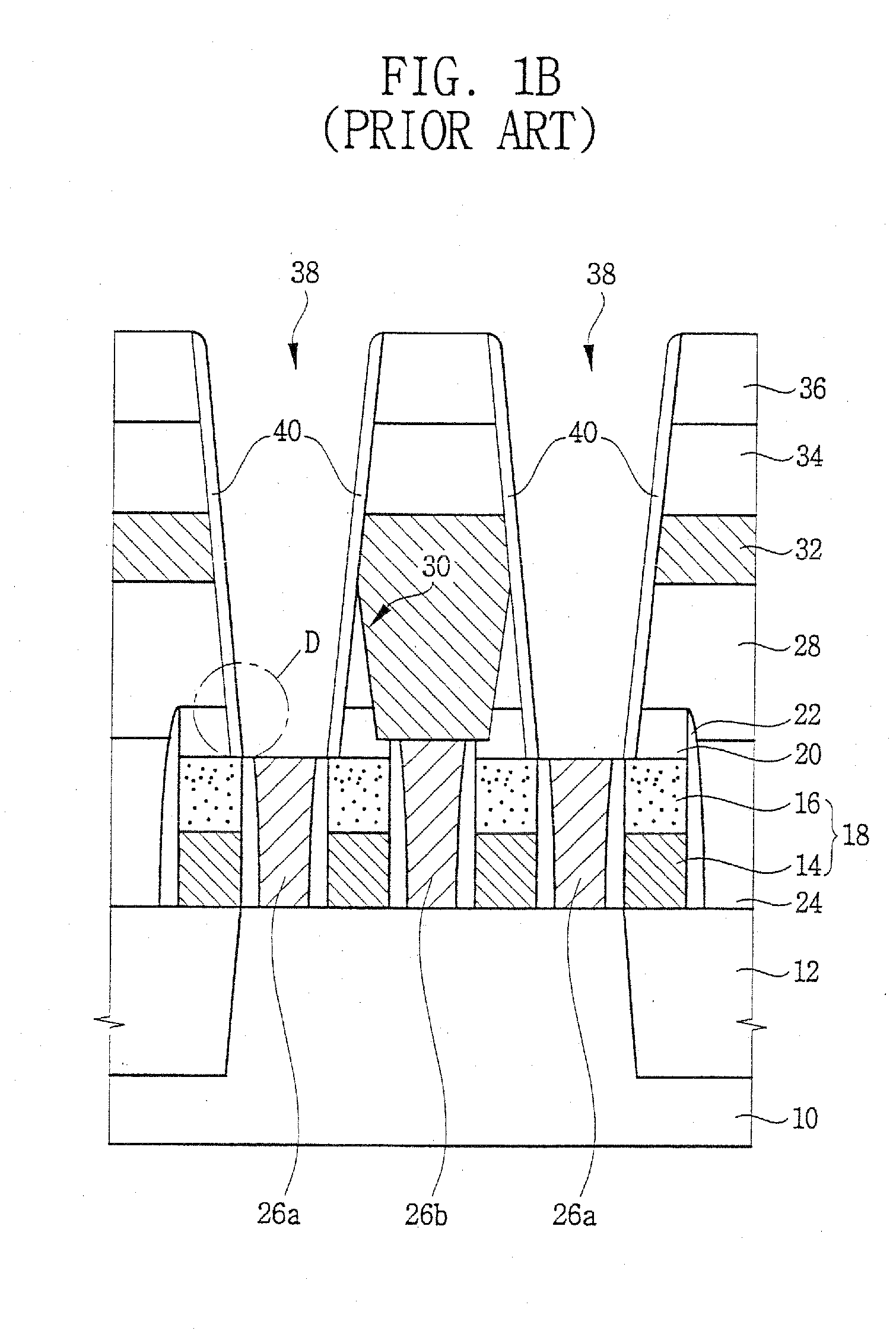
[0030] Referring to FIG. 2A, a plurality of wirings 55 is formed on a semiconductor substrate 50. The wirings 55 are separated from one another. Each of the wirings 55 includes a first conductiv...


PUM


Abstract

Wirings including first conductive layer patterns and insulating mask layer patterns are formed on a substrate. Insulating spacers are formed on sidewalls of the wirings. Self-aligned contact pads including portions of a second conductive layer are formed to contact with surfaces of the insulating spacers and to fill up a gap between the wirings. An interlayer dielectric layer is formed on the substrate where the contact pads are formed and is then partially etched to form contact holes exposing the contact pads. A selective epitaxial silicon layer is formed on the contact pads exposed through the contact holes to cover the insulating mask layer patterns. Thus, a short-circuit between the lower wiring and an upper wiring formed in the contact holes is prevented.

Description

CROSS REFERENCE TO RELATED APPLICATION [0001] This is a Divisional of U.S. patent application Ser. No. 10 / 688,017, filed on Oct. 16, 2003, now pending, which claims priority from Korean Patent Application No. 2003-4358, filed on Jan. 22, 2003, the contents of which are incorporated by reference.BACKGROUND OF THE INVENTION [0002] 1. Field of the Invention [0003] This disclosure relates to a semiconductor device, and more particularly, to a dynamic random access memory (DRAM) and a method of manufacturing the same. [0004] 2. Description of the Related Art [0005] As techniques for manufacturing semiconductor devices develop and the applications for memory devices expand, memory devices having large capacities are required. In particular, the integration density of a DRAM device, wherein a memory cell is composed of one capacitor and one transistor, has remarkably improved. [0006] As the integration density of semiconductor device increases, the size of contact hole connecting one eleme...

Claims


Application Information

Patent Timeline
Patent Type & Authority Applications(United States)
IPC IPC(8): H01L23/52H01L21/28H01L21/60H01L21/768H01L21/8242H01L27/02H01L27/108
CPCH01L21/76831H01L21/76877H01L21/76895H01L21/76897H01L27/0207H01L27/10814H01L2924/0002H01L27/10855H01L27/10888H01L2924/00H10B12/315H10B12/485H10B12/0335H10B12/00
Inventor PARK, BYUNG-JUNKIM, JI-YOUNG
Owner SAMSUNG ELECTRONICS CO LTD
Why Eureka
Try Eureka