
Eureka
For R&D, Eureka makes reading and utilizing patents & technical documents easy.
Eureka AIR
Designed for self-driven R&D workflows. Generate viable solutions, solve complex R&D challenges, empower your innovation with AI.

Eureka Materials
Designed for material experts only. Revolutionize your material R&D, from search, analyze, to developing new materials.

TechResearch
Generate reliable direction feasibility study reports for your R&D in just a few steps.

TechSeek
Discover and master advanced knowledge NOW. Basics, ideas, possibilities, all at once.

TechMind
As an expert in R&D Theories, TechMind can generates customized viable solutions instantly.

TechRisk
Analyze your overall solution with one click, know your potential R&D risks in advance.

TechMonitor
Get weekly tech updates, stay abreast of the latest tech innovations and key insights.
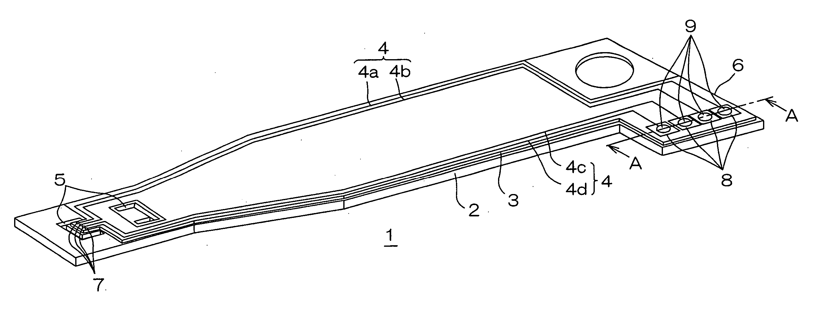
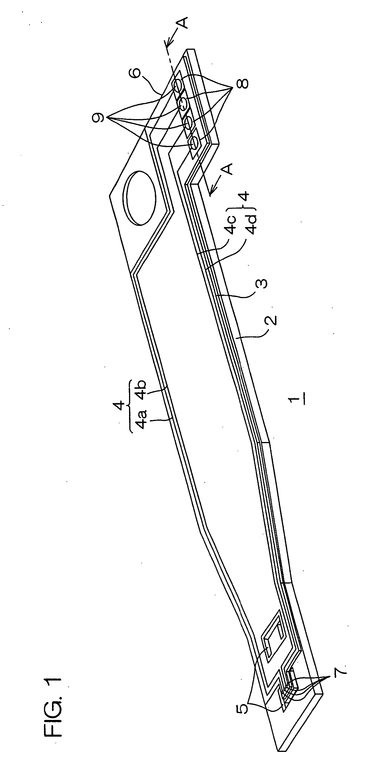
Wired circuit board
- Summary
- Abstract
- Description
- Claims
- Application Information
AI Technical Summary
Benefits of technology
Problems solved by technology
Method used
Image

Examples
example 1
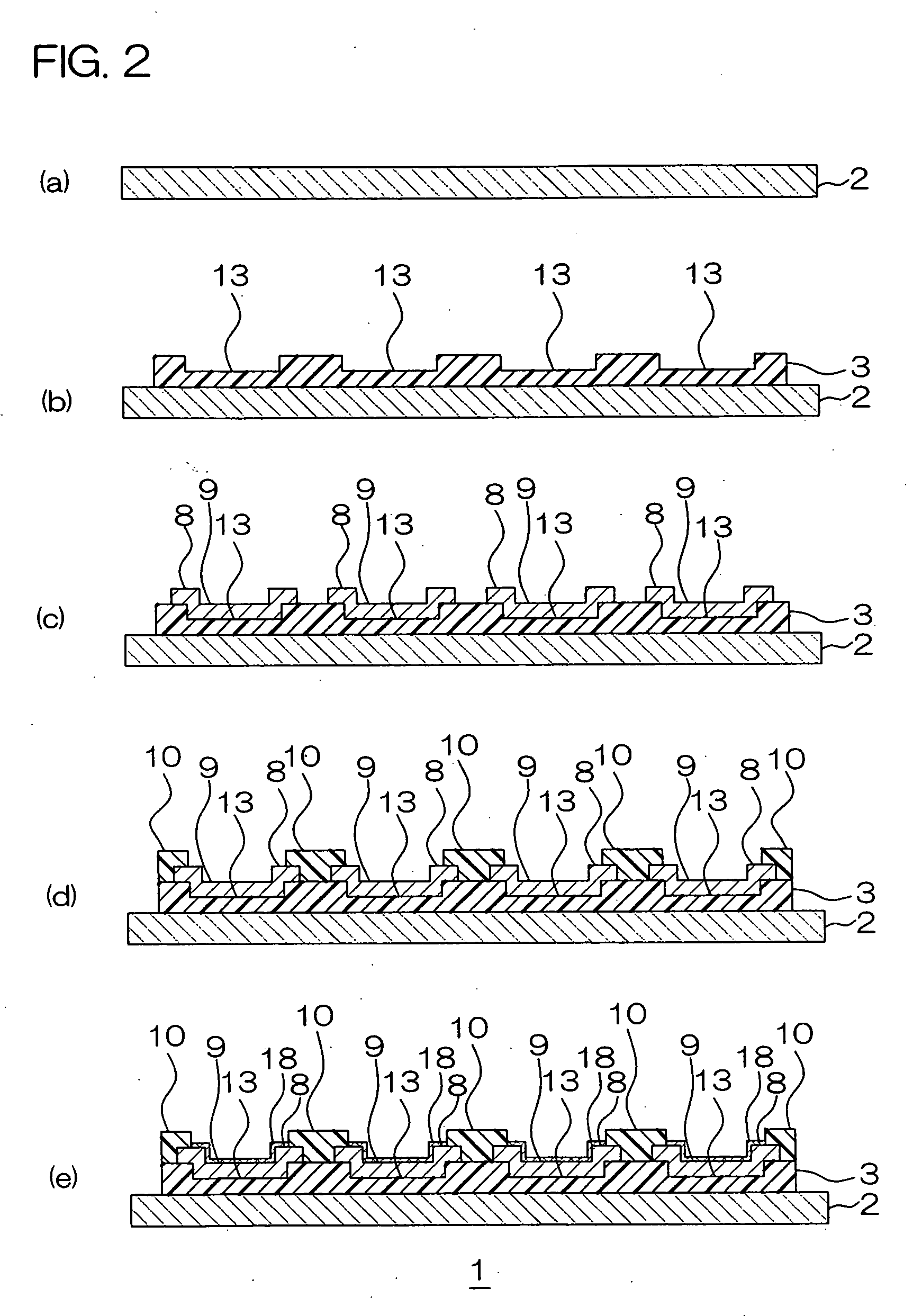
[0114] The supporting board 2 of a stainless foil (SUS304) of 300 mm wide and 25 μm thick was prepared (Cf. FIG. 2(a)).
[0115] Then, after solution of precursor of photosensitive polyimide resin (photosensitive polyamic acid resin) was coated over the entire surface of the supporting board 2, the coated resin was heated for two minutes at 120° C. , to form a coating 11 of the precursor of the photosensitive polyimide resin (Cf. FIG. 3(a)).
[0116] Thereafter, the photomask 12 was disposed opposite the coating 11 so that that the light shielding portions 12a confronted portions of the coating 11 where the insulating base layer 3 was not to be formed on the supporting board 2; the total-light-transmitting portions 12b confronted portions of the coating 11 where the insulating base layer 3 was to be formed on the supporting board 2; and the semi-light-transmitting portions 12c confronted portions of the coating 11 where the conductive concave portions 9 were to be formed in the respecti...
PUM
 Abstract
Description
Claims
Application Information
 - R&D Engineer
- R&D Manager
- IP Professional
- Industry Leading Data Capabilities
- Powerful AI technology
- Patent DNA Extraction
Browse by: Latest US Patents, China's latest patents, Technical Efficacy Thesaurus, Application Domain, Technology Topic, Popular Technical Reports.
© 2024 PatSnap. All rights reserved.Legal|Privacy policy|Modern Slavery Act Transparency Statement|Sitemap|About US| Contact US: help@patsnap.com