Solid-state image pickup device and drive method thereof
Inactive Publication Date: 2006-09-14
SONY CORP
View PDF6 Cites 223 Cited by
Summary
Abstract
Description
Claims
Application Information
AI Technical Summary
This helps you quickly interpret patents by identifying the three key elements:
Problems solved by technology
Method used
Benefits of technology
Benefits of technology
[0018] In the solid state imaging apparatus or the driving method therefor with the constitution described above, at the time of pixel skipping and readout, pixel information of a same color filter in the unit pixel block is outputted as pixel information for one pixel simulatively, whereby a distance between pixels increases simulatively and a pixel area increases simulatively. Consequently, an MTF value falls in a spatial frequency domain equal to or higher than the Nyquist frequency. As a result, aliasingnoise decreases.
Image
Click on the blue label to locate the original text in one second.
Reading with bidirectional positioning of images and text.
Examples
first embodiment
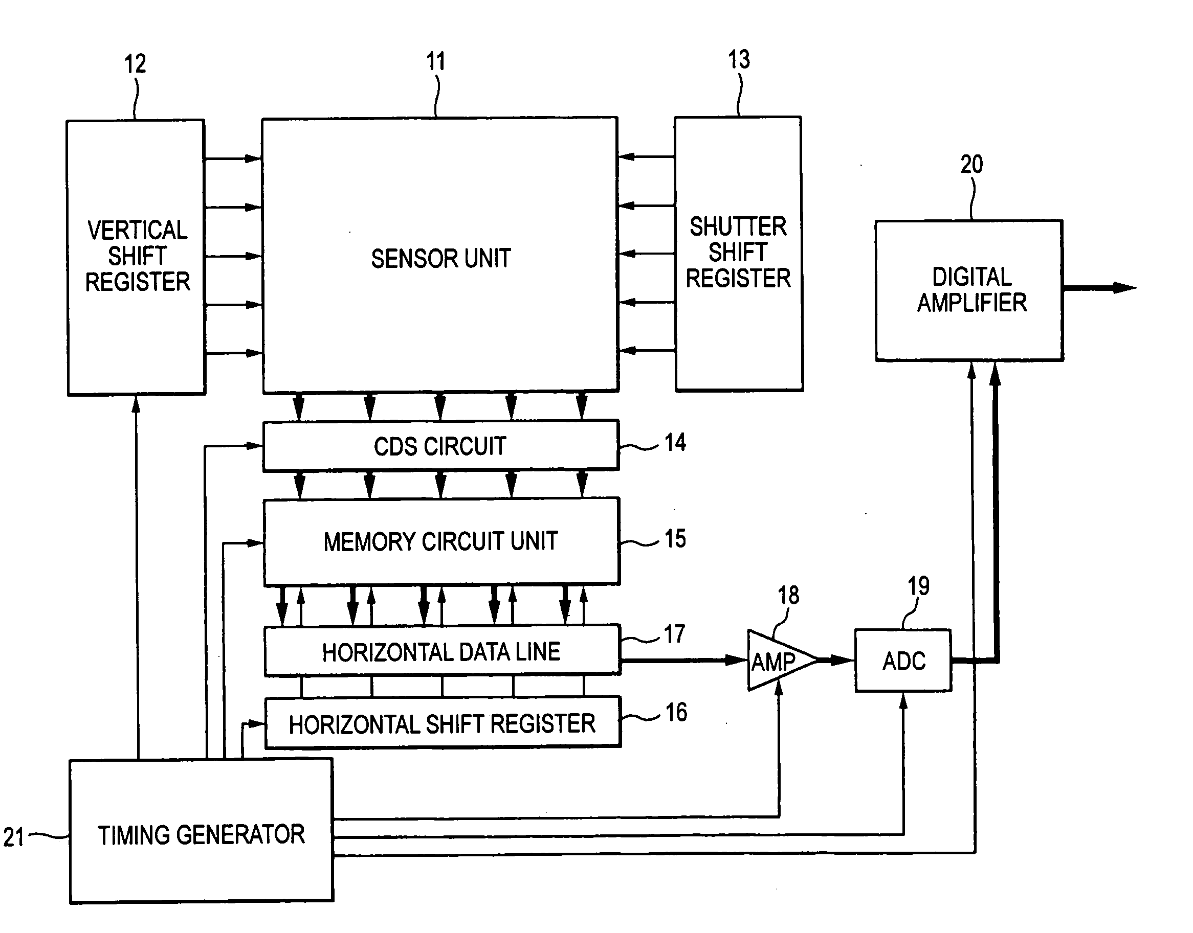
[0051]FIG. 1 is a block diagram showing an example of a constitution of a solid state imaging apparatus according to a first embodiment of the invention. In an example explained in this embodiment, an X-Y addressable solid state imaging apparatus of a type for reading out information of pixels for one row simultaneously, for example, a CMOS image sensor is used as a solid state imaging apparatus.
[0053] The sensor unit 11 has a constitution in which pixels are arranged in a matrix shape and row selection lines, shutter lines, vertical data lines, and the like are wired with res...
second embodiment
[0084] A constitution of a solid state imaging apparatus according to a second embodiment of the invention is basically the same as that of the solid state imaging apparatus according to the first embodiment shown in FIG. 1. However, in the solid state imaging apparatus according to this embodiment, when k is a positive integer equal to or larger than 0, in a process of compressing an amount of pixel information at a ratio of 1 / (k+2)×(k+2), (k+2)×(k+2) pixels are skipped and added in a state in which simulative pixel blocks (unit pixel blocks) to be skipped and added are laid to overlap one another, whereby the pixel information is skipped in a state in which aliasing noise is reduced. The solid state imaging apparatus in this embodiment will be explained citing specific examples.
FIRST SPECIFIC EXAMPLE
[0085] In a case of a first specific example, k=0, in other words, four (2×2) pixels are skipped and added and an amount of pixel information is compressed at a ratio of 1 / 4. This ca...
fourth specific example
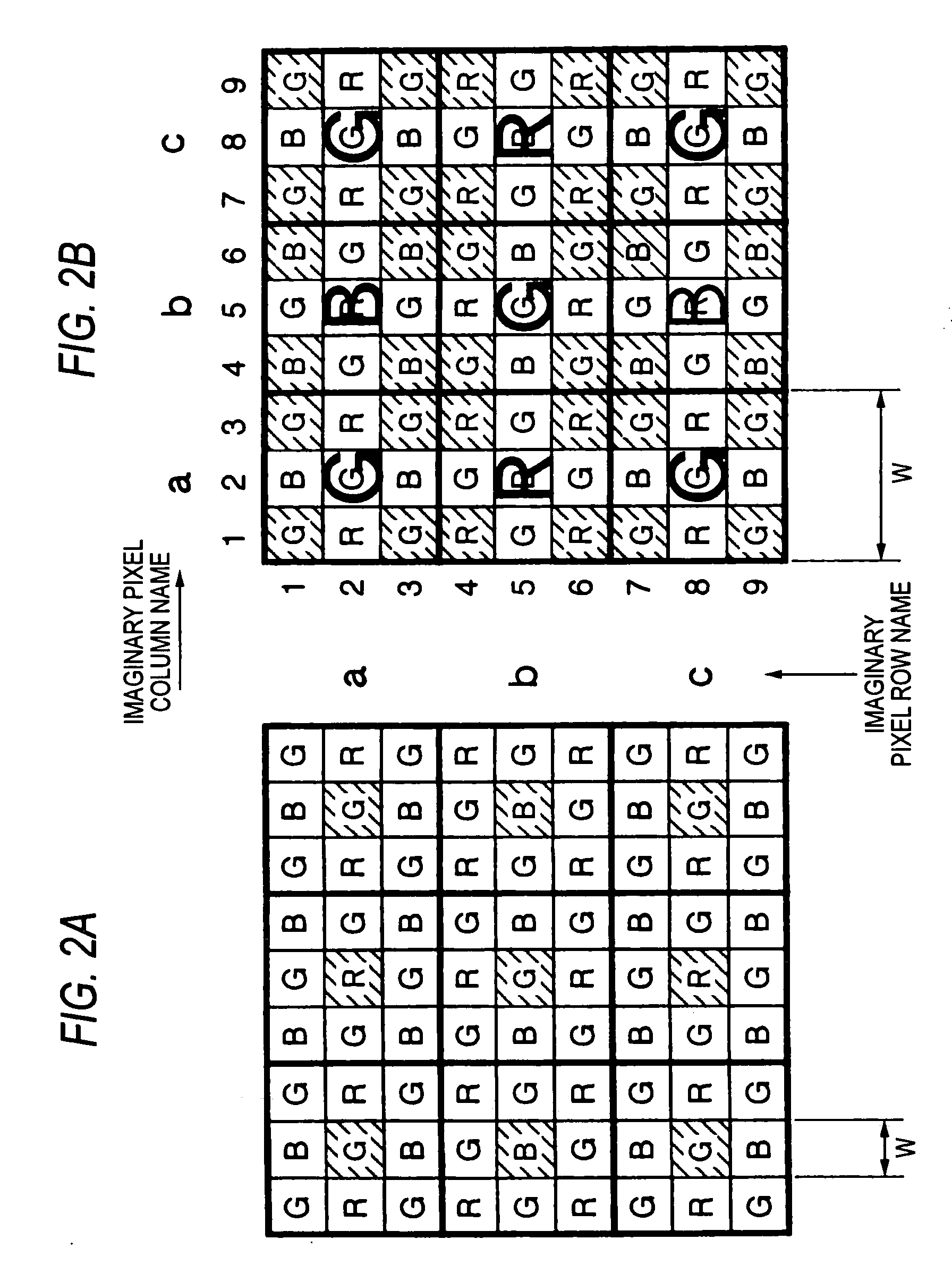
[0102] In a case of a fourth specific example, k=3, in other words, twenty-five (5×5) pixels are skipped and added and an amount of pixel information is compressed at a ratio of 1 / 25. This case will be explained with reference to diagrams for explaining operations in FIGS. 14A to 14D.
[0103] First, as shown in FIG. 14A, pieces of pixel information in first, third, fifth, seventh, and ninth columns of first, third, fifth, seventh, and ninth rows are added and outputted as information for one pixel. Next, as shown in FIG. 14B, pieces of pixel information in sixth, eighth, tenth, twelfth, and fourteenth columns of the first, the third, the fifth, the seventh, and the ninth rows are added and outputted as information for one pixel. Similarly, pieces of pixel information in eleventh, thirteenth, fifteenth, seventeenth, and nineteenth columns of the first, the third, the fifth, the seventh, and the ninth rows are added and outputted as information for one pixel.
[0104] When the same opera...
PUM
Abstract
When pixels are simply skipped while keeping both an order of pixel information and a spatial positional relation the same as those in all-pixel readout, since a distance between pixels to be read out increases, the Nyquist frequency decreases and aliasingnoise increases. A 5×5 pixel block is set as a unit pixel block and pieces of pixel information in first, third, and fifth columns of first, third, and fifth rows of a pixel arrangement are added and outputted as an output in an ath row and an ath column of the unit pixel block. Then, pieces of pixel information in sixth, eighth, and tenth columns of the first, the third, and the fifth rows of the pixel arrangement are added and outputted as an output in the ath row and a bth column of the unit pixel block. Subsequently, pieces of pixel information are added and outputted up to a last column or a column near the last column. Thereafter, pieces of pixel information in the first, the third, and the fifth columns of the sixth, the eighth, and the tenth rows of the pixel arrangement are added and outputted as an output in a bth row and the ath column of the unit pixel block. Subsequently, all arbitrary pixels are read out while repeating the same operation and skipping and adding pieces of pixel information.
Description
TECHNICAL FIELD [0001] The present invention relates to a solid state imaging apparatus and a driving method therefor, and more particular to a solid state imaging apparatus using an X-Y addressable solid state imaging apparatus and a driving method therefor. BACKGROUND ART [0002] A solid state imaging apparatus is roughly divided into a charge transfer solid state imaging apparatus represented by, for example, a CCD (Charge Coupled Device) image sensor and an X-Y addressable solid state imaging apparatus represented by, for example, a CMOS (Complementary MetalOxideSemiconductor) image sensor. This type of solid state imaging apparatus is used in various video apparatuses such as a video camera for photographing moving images and an electronic still camera for photographing still images as an imaging apparatus therefor. [0003] Conventionally, when the CCD image sensor is used as an imaging apparatus in a 1CCD color camera, in a so-called pixel skipping processing for skipping pixe...
Claims
Application Information
Patent Timeline
Application Date:The date an application was filed.
Publication Date:The date a patent or application was officially published.
First Publication Date:The earliest publication date of a patent with the same application number.
Issue Date:Publication date of the patent grant document.
PCT Entry Date:The Entry date of PCT National Phase.
Estimated Expiry Date:The statutory expiry date of a patent right according to the Patent Law, and it is the longest term of protection that the patent right can achieve without the termination of the patent right due to other reasons(Term extension factor has been taken into account ).
Invalid Date:Actual expiry date is based on effective date or publication date of legal transaction data of invalid patent.

