Multilayer printed wiring board

Inactive Publication Date: 2010-02-16
MITSUBISHI ELECTRIC CORP
View PDF6 Cites 5 Cited by
  • Summary
  • Abstract
  • Description
  • Claims
  • Application Information

AI Technical Summary

Benefits of technology

[0011]According to the multilayer printed wiring board of the present invention, two power supply patterns with the same power supply voltage are formed on the power supply layer in a non-contact manner with each other, and the two power supply patterns are electrically connected to each other via a relay portion including the relay pattern formed on a condu

Problems solved by technology

Therefore, there is a problem in that the 3.3 V power supply pattern is lengthened, the impedance is in

Method used


Image

  • Multilayer printed wiring board
  • Multilayer printed wiring board
  • Multilayer printed wiring board

Examples


Example

Embodiment 1

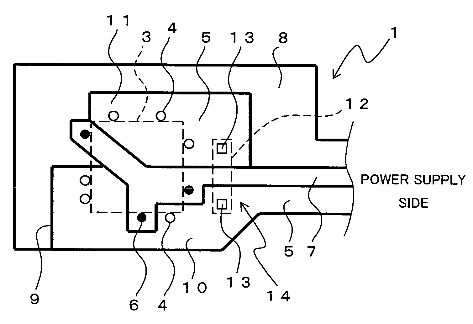
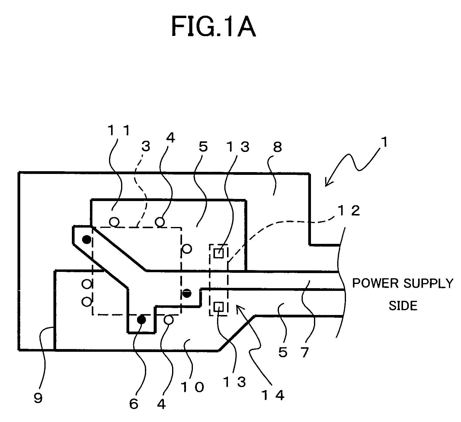
[0019]FIG. 1A is a plan view illustrating a power supply layer 1 of a multilayer printed wiring board according to Embodiment 1 of the present invention, and FIG. 1B is a plan view illustrating a signal layer 2 (conductor layer) of the multilayer printed wiring board according to Embodiment 1 of the present invention. It is to be noted that the actual power supply layer 1 and signal layer 2 are provided with other members and portions than those described below but illustration and description thereof are omitted.

[0020]In FIGS. 1A and 1B, a 5 V power supply pattern 5 for supplying power to 5 V power supply pins 4 (white circles in the figures) of an IC 3 mounted on the signal layer 2, a 3.3 V power supply pattern 7 for supplying power to 3.3 V power supply pins 6 (black circles in the figures) of the IC 3, and, for example, a 1.2-V power supply pattern 8 serving as another power supply voltage for supplying power to a member which is not shown are formed in the power sup...

Example

Embodiment 2

[0031]FIG. 2 is a plan view illustrating a power supply layer 1 of a multilayer printed wiring board according to Embodiment 2 of the present invention.

[0032]In FIG. 2, a 5 V power supply pattern 5, a 3.3 V power supply pattern 7, and a 1.2-V power supply pattern 8 are formed on the power supply layer 1 so as to be insulated from each other via boundary portions 9.

[0033]Here, the 3.3 V power supply pattern 7 has a first pattern portion 15 and a second pattern portion 16 which are formed in a non-contact manner with each other.

[0034]A relay pattern 12 made of the same material as that of the first and second pattern portions 15 and 16 is formed in a signal layer 2. Except for this, the structure is the same as that of Embodiment 1, and thus, description thereof is omitted.

[0035]An operation of the multilayer printed wiring board structured as above is now described hereinafter.

[0036]The 3.3 V power supply voltage supplied to the first pattern portion 15 is also supplied t...

Example

Embodiment 3

[0041]While, in Embodiment 2 described in the above, attention is focused on the power supply voltages of the respective power supply patterns, here, another embodiment is described where attention is focused on pattern widths which are lengths in a direction perpendicular to the direction of flow of electric current through the respective power supply patterns.

[0042]Generally, when a power supply pattern has a portion where the pattern width is small, according to the difference in the pattern widths at a connecting point of the portion where the pattern width is small and other portions, the impedance at the connecting point is increased, and thus, large noise is generated at the connecting point.

[0043]This embodiment has been made to solve the problem described in the above.

[0044]FIG. 3 is a plan view illustrating a power supply layer 1 of a multilayer printed wiring board according to Embodiment 3 of the present invention. FIG. 4 is another plan view illustrating a p...


PUM


Abstract

Provided is a multilayer printed wiring board in which power supply patterns are shortened to decrease an impedance and electromagnetic radiation noise. The multilayer printed wiring board includes: a power supply layer (1) having at least two power supply patterns (5) with different voltages formed thereon; and a conductor layer (2) overlaid on the power supply layer (1) via an insulator, and at least one of the power supply patterns (5) has a first pattern portion (10) and a second pattern portion (11) formed in a non-contact manner with each other, and the first pattern portion (10) and the second pattern portion (11) are electrically connected to each other via a relay portion (14) including a relay pattern (12) formed on the conductor layer (2) and through holes (13) for connecting the power supply layer (1) and the conductor layer (2) at both ends of the relay pattern (12).

Description

BACKGROUND OF THE INVENTION[0001]1. Field of the Invention[0002]The present invention relates to a multilayer printed wiring board provided with a power supply layer having a plurality of power supply patterns with different power supply voltages.[0003]2. Description of the Related Art[0004]A conventional multilayer printed wiring board generally has a structure including at least one signal layer, at least one power supply layer, and at least one ground layer. Since power supply voltage used in a power supply layer in electronic equipment having a conventional digital circuit is mainly 5 V, a single 5 V power supply pattern is formed in the power supply layer in many cases.[0005]In a conventional printed circuit board, a connector to which power is supplied is arranged in proximity to an LSI (large scale integration) the power consumption of which is highest on the board. Further, a power supply pattern formed from the power supply connector to an area where the LSI with the highes...

Claims


Application Information

Patent Timeline
IPC IPC(8): H05K1/14
CPCH05K1/0262H05K1/0298H05K2201/093H05K2201/09663H05K2201/10689
Inventor GOTOU, SHIGETADAASAO, YOSHIHITO
Owner MITSUBISHI ELECTRIC CORP
Why Eureka
Try Eureka