Bias Circuit

Inactive Publication Date: 2008-02-28
MITSUBISHI ELECTRIC CORP
View PDF5 Cites 4 Cited by
  • Summary
  • Abstract
  • Description
  • Claims
  • Application Information

AI Technical Summary

Benefits of technology

[0019] According to an aspect of the invention, an impedance component of a parallel circuit made up of an inductor provided in a bias circuit and an impedance decreasing prevention element has not only an inductive reactance component but also

Problems solved by technology

In the approach of using the short stub of a quarter-wave length as disclosed in the patent document 1, however, a problem arises in that the stub can be used in an amplifying circuit that amplifies a signal whose spectrum is concentrated near a clock frequency, but can not be used in an amplifying circuit that amplifies a baseband signal that has a wide range of spectrum component.
The approach of using a resistor that has a substantially larger impedance than that in a transmission line as disclosed in the patent document 2 has a problem in that, for example, when applying bias voltage to a terminal necessary for current to be supplied such as a drain terminal, though the approach is rather easy to accommodate a tendency to growing broadband based on an original property of a resistor that fundamentally has a broadband property, it is necessary to apply bias voltage to which an amount of voltage drop in the resistor is added, thereby causing larger power source voltage.
In the approach disclosed in the non-patent

Method used


Image

  • Bias Circuit
  • Bias Circuit
  • Bias Circuit

Examples


first embodiment

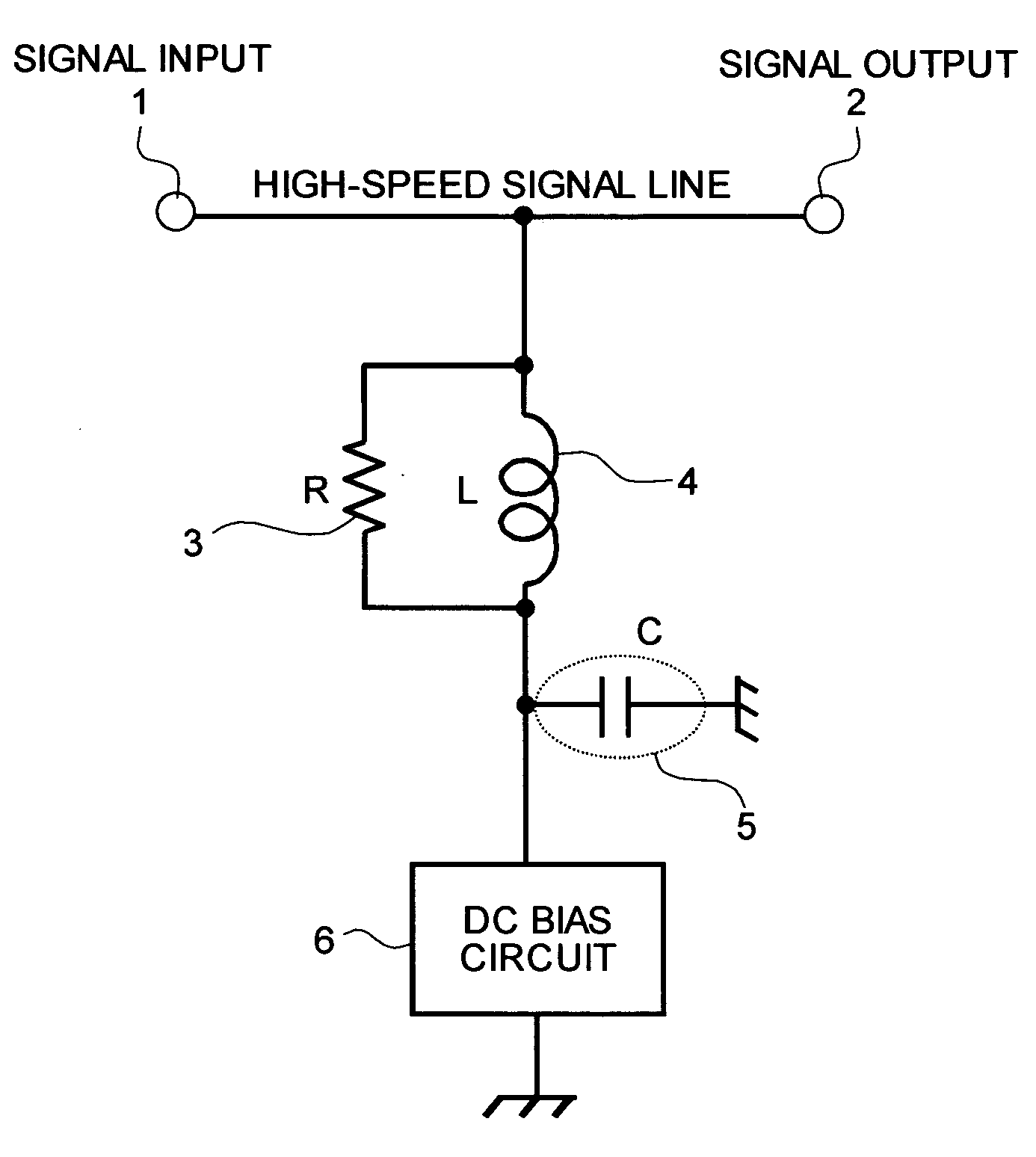
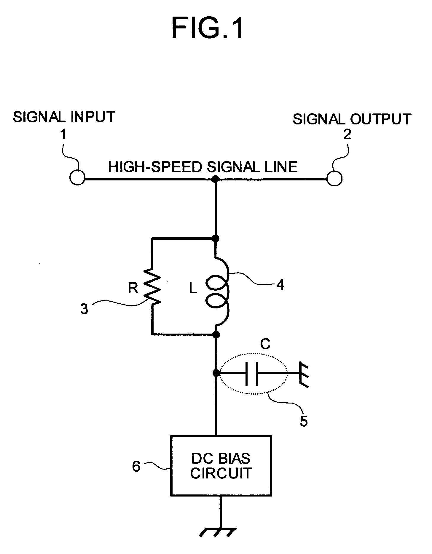
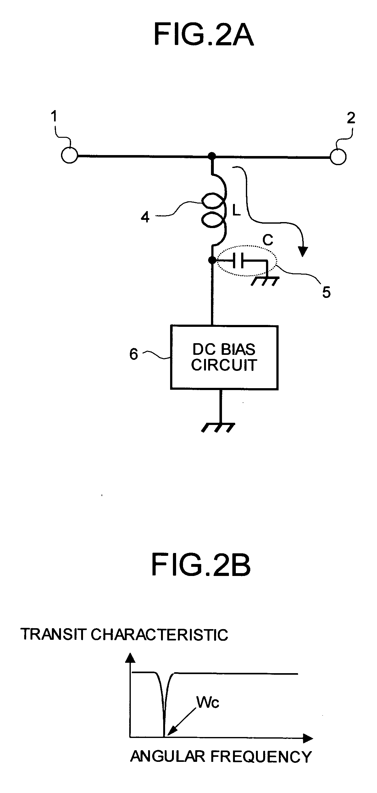
[0035]FIG. 1 is a circuit diagram of the bias circuit according to a first embodiment of the present invention. The bias circuit shown in FIG. 1 is configured, for example, to supply bias voltage (or bias current, hereinafter, referred to “bias power source”) to one end of a high-speed signal line having a signal input end 1 and a signal output end 2. In FIG. 1, the bias power source output from a DC bias circuit 6 constituted by a conventional art is supplied to one end of the high-speed signal line through a parallel circuit including a resistance element 3 and an inductor 4. The inductor 4 is for blocking the above-described AC signal. A capacitor 5 is a parasitic capacitance generated between the mounting pattern and a ground potential. One end of the capacitor 5 is connected to one end of the parallel circuit composed of the resistance element 3 and the inductor 4, and the other end is grounded by connecting to a ground.

[0036] Next, an explanation will be given about an operat...

second embodiment

[0052]FIG. 6 is a circuit diagram of a bias circuit according to a second embodiment of the present invention. In the bias circuit shown in FIG. 6, a resistance element 3a is serially connected to the capacitor 5, which is a parasitic capacitance, instead of being connected to the inductor 4 in parallel in as in the bias circuit shown in FIG. 1. The other components in the second embodiment are the same or equivalent to that of the first embodiment and have been given the same numerals or signs.

[0053] Next, an explanation will be given about the operation of the bias circuit shown in FIG. 6. FIG. 7A is a schematic diagram of an impedance-frequency characteristic of the LCR resonance circuit in the bias circuit shown FIG. 6. FIG. 7B is a diagram of an impedance orbit in the LCR resonance circuit.

[0054] The LCR resonance circuit shown in FIG. 6 in which the resistance element 3 is serially connected to the capacitor 5 constitutes the LCR serial resonance circuit together with the in...

third embodiment

[0057]FIG. 8 is a circuit diagram of a bias circuit according to a third embodiment of the present invention. In the bias circuit shown in FIG. 8, a resistance element 3b is connected to the capacitor 5, which is a parasitic capacitance, not serially but in parallel in the bias circuit of the second embodiment as shown in 6. The other components in the third embodiment are the same or equivalent to that of the second embodiment and have been given the same numerals or signs.

[0058] Next, an explanation will be given about the operation of the bias circuit shown in FIG. 8. FIG. 9A is a schematic diagram of an impedance-frequency characteristic of the LCR resonance circuit in the bias circuit shown in FIG. 8. FIG. 9B is a diagram of an impedance orbit in the LCR resonance circuit. While the resistance element 3 is connected to the inductor 4 in parallel in the bias circuit shown in FIG. 1, the resistance element 3b is connected to the capacitor 5 in parallel in the bias circuit shown ...


PUM


Abstract

A bias circuit that supplies bias voltage or bias current to one end of a transmission line includes an inductor that prohibits a high frequency component of a baseband signal transmitted on the transmission line and passes a frequency component near direct current of the baseband signal, and an impedance-decrease prevention element that prevents impedance from decreasing, when viewed from the transmission line, that is produced due to a resonance between a parasitic capacitance generated due to the inductor and an inductance of the inductor.

Description

TECHNICAL FIELD [0001] The invention relates to a bias circuit and particularly to a bias circuit that applies direct current (DC) bias to a semiconductor element, an optical modulator, or the like that amplifies a signal, such as like a baseband signal, having a broad spectral component from a low frequency to a high frequency near DC. BACKGROUND ART [0002] A bias circuit that can be used in a communication device that deals with signals whose spectrums are concentrated near a clock frequency, such as in the microwave communication, has been disclosure in the patent document 1. In the patent document 1, a technique is implemented that a short stub having a length of a quarter wave of a clock frequency is used to realize a high impedance near a signal spectral frequency to thereby decreasing impedance in a positive manner with respect to other frequencies including DC. [0003] The patent document 2 discloses a technique for applying bias to a portion of high impedance, such as gate b...

Claims


Application Information

Patent Timeline
IPC IPC(8): H03F3/04H03F1/00H03F3/189H03H7/01H03H7/06H03H7/46H04B3/02H04B3/54
CPCH03F1/30H04B2203/5483H03H7/38H03F3/189
Inventor SHIMOMURA, KENKICHISUGIHARA, TAKASHISHIMIZU, KATSUHIRO
Owner MITSUBISHI ELECTRIC CORP
Why Eureka
Try Eureka