Electrode structure of organic electroluminescent display panel and method of manufacturing the same

Inactive Publication Date: 2006-02-23
UNIVISION TECHNOLOGY
View PDF0 Cites 1 Cited by
  • Summary
  • Abstract
  • Description
  • Claims
  • Application Information

AI Technical Summary

Benefits of technology

[0006] It is a primary object of the present invention to provide an electrode structure of an organic electroluminescent display panel and a method of manufacturing the same which uses an electrode isolation layer to make external leading wire area without additionally

Problems solved by technology

Even if the organic electroluminescence is a burgeoning technology currently, quite a bit difficulty are encountered in real applications, including: stability of maintaining light emitting in a very short time and difficulty of light emitting efficiency came from larger panels, waterproof packages came from the organic materials themselves and usage lifetime problems, non-uniformity of light emitti

Method used


Image

  • Electrode structure of organic electroluminescent display panel and method of manufacturing the same
  • Electrode structure of organic electroluminescent display panel and method of manufacturing the same
  • Electrode structure of organic electroluminescent display panel and method of manufacturing the same

Examples


first embodiment

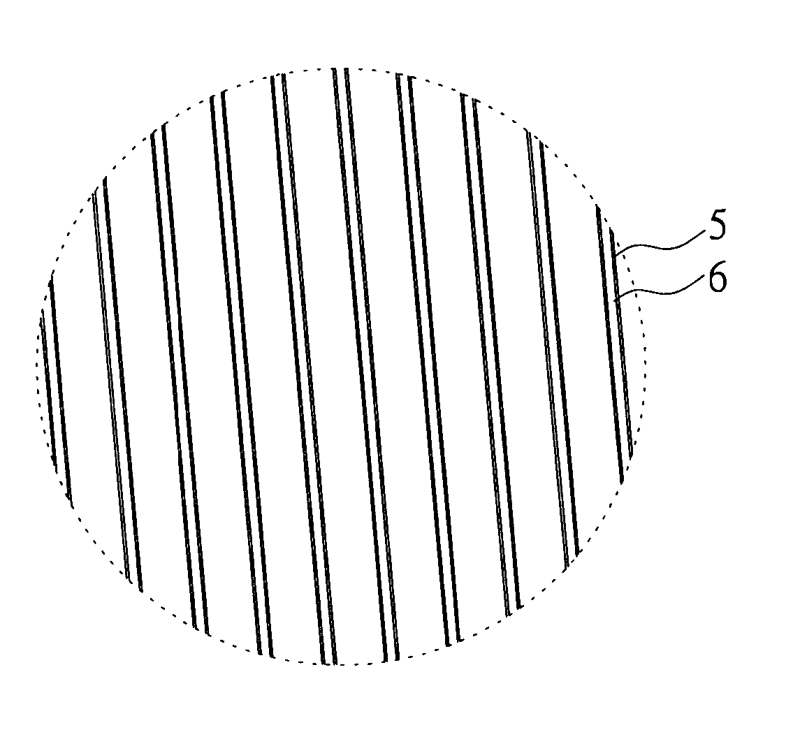
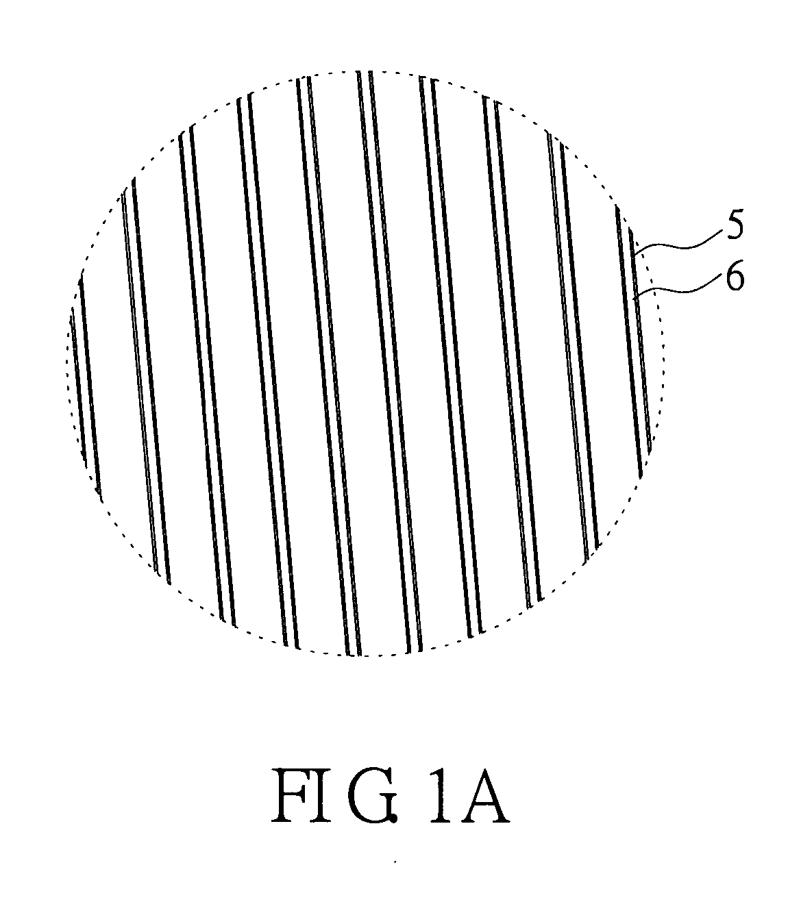
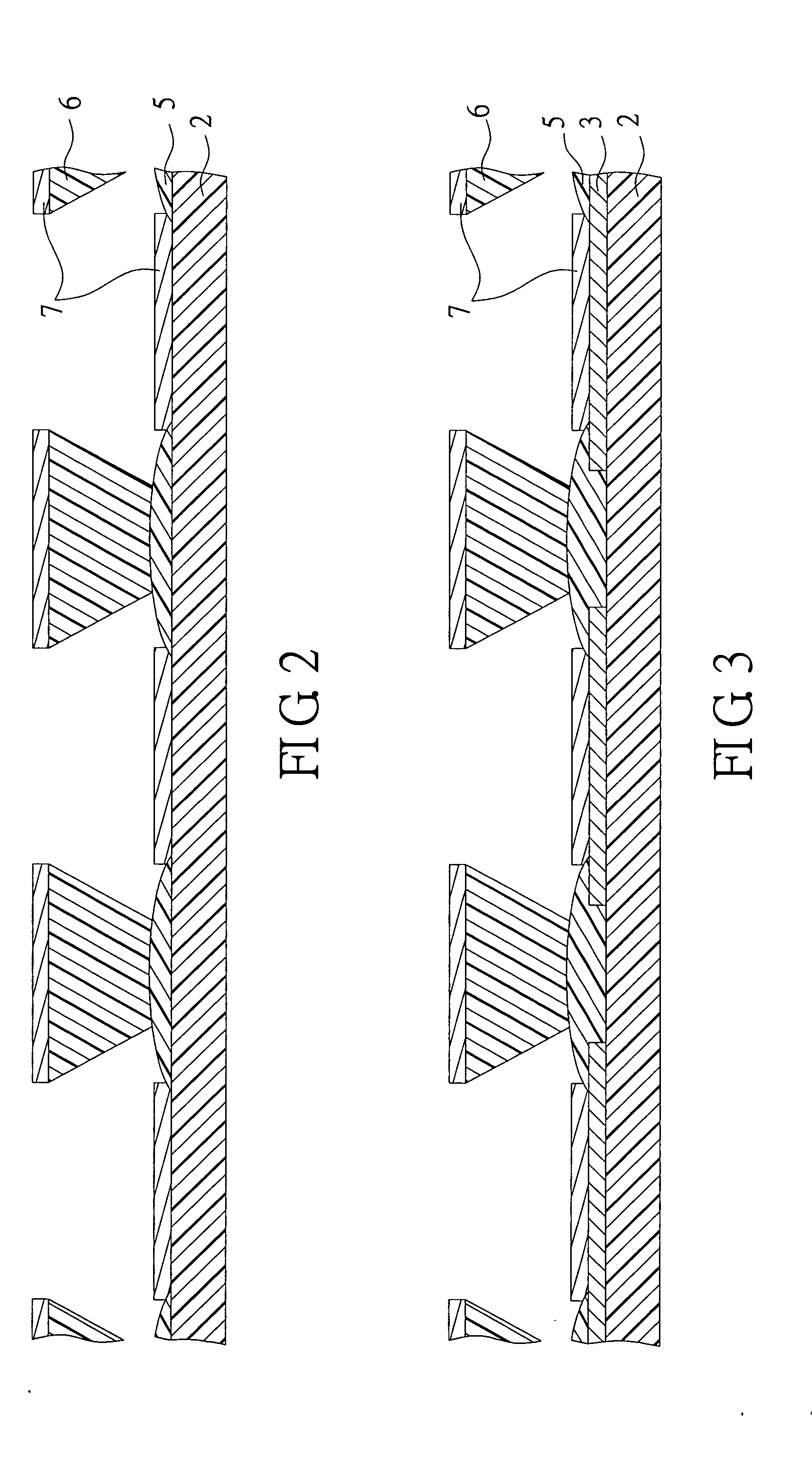
[0021] the electrode structure of the organic electroluminescent display panel 10 of the present invention as shown in FIG. 2 comprises a transparency substrate 2, an isolation area 5 provided on the transparency substrate 2 as isolation, a separation area 6 provided on the isolation area 5 with a raised predetermined height to separate electrical interference, and at least one metallic conductive layer 7 provided on the transparency substrate 2 and the separation area 6. The isolation area 5 isolates the electrical connection of adjacent leading wires. The separation area 6 with the predetermined height separates from and electrically isolates the metallic conductive layers 7 respectively provided on the separation area 6 and the transparency substrate 2 and further avoids from electrical interference of adjacent leading wires. Besides, the at least one metallic conductive layer 7 on the separation area 6 and the at least one metallic conductive layer 7 on the transparency substrat...

second embodiment

[0022] the electrode structure of the organic electroluminescent display panel 10 of the present invention as shown in FIG. 3 comprises a transparency substrate 2, a leading wire pattern layer 3 provided on the transparency substrate 2, an isolation area 5 provided on the leading wire pattern layer 3 as isolation, a separation area 6 provided on the isolation area 5 with a raised predetermined height to separate electrical interference, and at least one metallic conductive layer 7 provided on the leading wire pattern layer 3 and the separation area 6. The isolation area 5 isolates the electrical connection of adjacent leading wires. The separation area 6 with the predetermined height separates from and electrically isolates the metallic conductive layers 7 respectively provided on the separation area 6 and the leading wire pattern layer 3 and further avoids from electrical interference of adjacent leading wires. Besides, the at least one metallic conductive layer 7 on the separation...

third embodiment

[0023] the electrode structure of the organic electroluminescent display panel 10 of the present invention as shown in FIG. 4 comprises a transparency substrate 2, a leading wire pattern layer 3 provided on the transparency substrate 2, at least one auxiliary metallic conductive layer 4 provided on the leading wire pattern layer 3, an isolation area 5 provided on the leading wire pattern layer 3 as isolation, a separation area 6 provided on the isolation area 5 with a raised predetermined height to separate electrical interference, and at least one metallic conductive layer 7 provided on the auxiliary metallic conductive layer 4 and the separation area 6. The isolation area 5 isolates the electrical connection of adjacent leading wires. The separation area 6 with the predetermined height separates from and electrically isolates the at least one metallic conductive layer 7 provided on the separation area 6 and the at least one metallic conductive layer 7 provided on the auxiliary met...


PUM

PropertyMeasurementUnit
Electrical conductoraaaaaaaaaa
Metallic bondaaaaaaaaaa
Transparencyaaaaaaaaaa

Abstract

An electrode structure of an organic electroluminescent display panel and a method of manufacturing the same are provided. The electrode structure comprises a transparency substrate, a leading wire pattern layer (for example: ITO, IZO or IWO materials etc.) grown on the transparency substrate, at least one auxiliary metallic pattern layer grown on the leading wire pattern layer, an isolation area provided on the auxiliary metallic pattern layer for isolation, a separation area provided on the isolation area with an raised predetermined height to separate electric interference, and at least one metallic conductive layer provided on the transparency substrate and the separation area. By the separation area with the predetermined height separating apart and electrically isolating the metallic conductive layers respectively provided on the separation area and the auxiliary metallic pattern layer, the at least one metallic conductive layer on the separation area, the at least one metallic conductive layer on the auxiliary metallic pattern layer or the leading wire pattern layer, the auxiliary metallic pattern layer, and/or the leading wire pattern layer are in a series connection to reduce the electrode impedance.

Description

FIELD OF THE INVENTION [0001] The present invention is related to an organic electroluminescent display panel and more particularly to an organic electroluminescent display panel with an external electrode leading wire with low impedance. BACKGROUND [0002] Organic electroluminescence means a phenomenon using injection and compound of carriers to cause light emitting driven by an electric current. The principle is respectively using transparent electrodes made of ITO, IZO or IWO etc. materials and metallic electrodes as an anode and cathode of elements. Under a certain voltage driving, electrons and holes respectively inject to electronic and hole transport layers from the cathode and anode such that the electrons and the holes are moved to light emitting layer respectively through the electronic and hole transport layers and met in the light emitting layer to make light emitting molecules arouse visible light. The technical features of the organic electroluminescence comprises: self...

Claims


Application Information

Patent Timeline
IPC IPC(8): H01J1/62B32B19/00H01L27/32H01L51/52H05B33/06
CPCH01L27/3283H01L51/5212H01L51/5203H01L27/329H10K59/173H10K59/1795H10K50/814H10K59/805H10K50/805
Inventor LAN, WEN-JENGCHANG CHIEN, CHIN CHUNGLEE, MING TEYU, HUI-CHANGCHIEN, TING CHIEH
Owner UNIVISION TECHNOLOGY
Why Eureka
Try Eureka