Apparatus adapted to engrave a label and related method

Inactive Publication Date: 2006-09-21
SAMSUNG ELECTRONICS CO LTD
View PDF25 Cites 0 Cited by
  • Summary
  • Abstract
  • Description
  • Claims
  • Application Information

AI Technical Summary

Benefits of technology

[0017] Embodiments of the present invention provide a method of effectively engraving a label by maintaining an energy level of a laser beam at a constant level. Embodiments of the present invention also provide an apparatus for performing the method.

Problems solved by technology

However, this conventional approach to the formation of labels on wafers suffers from a number of problems.
However, where the light is improperly applied to form label L, abnormal dots, like dot D2 in FIG. 3, are formed.
However, the formation of an abnormal dot generally occurs when the light applied to wafer W has an energy level ill-suited (e.g., too high, wrong frequency, etc.) to the task of forming the label.
However, when abnormal dots D2 are formed on the wafer, its surface may be fractured, thereby producing minute particles.
Thereafter, when the wafer is polished in a chemical mechanical polishing (CMP) process, for example, these particles may scratch and further damage the wafer surface.
However, in both of these disclosures, the path of the engraving laser beam is merely controlled (e.g., partially changed or blocked) without any active control or even monitoring of the actual energy level of the laser beam.
As a result, failures in the formation of labels still occur due to variations in the temperature of the laser diode producing the engraving laser beam.
It should be noted that wafers, such as those for use as a semiconductor device substrate, are very expensive.
Thus, when a wafer damaged due to the problems associated with the formation of a label, a significant amount of time and money is lost.

Method used


Image

  • Apparatus adapted to engrave a label and related method
  • Apparatus adapted to engrave a label and related method
  • Apparatus adapted to engrave a label and related method

Examples


Embodiment Construction

[0027] Several example embodiments of the present invention will now be described with reference to the accompanying drawings. These embodiments are presented as teaching examples. The scope of the present invention is not limited to only the disclosed embodiments, but is defined by the following claims.

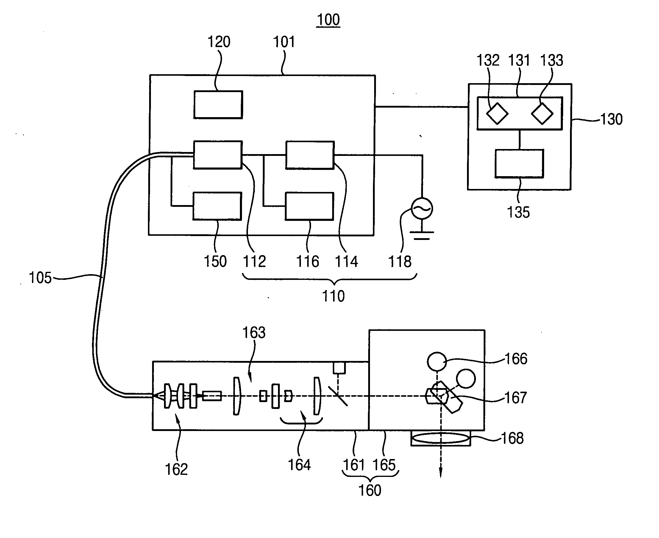
[0028]FIG. 4 is a perspective view illustrating a system adapted to engrave a label in accordance with an example embodiment of the present invention. FIG. 5 is a related schematic view further illustrating the system of FIG. 4.

[0029] In the illustrated example of FIGS. 4 and 5, an apparatus 100 adapted to engrave a label comprises a light source member 110, a measuring member 120, a processing member 130, a heat-exchanging member 150, and a projection member 160.

[0030] The light source member 110 is adapted to emit a laser beam, which is adapted to engrave a label on an object such as a semiconductor substrate. The light source member 110 comprises a laser diode 112, an internal ...


PUM

PropertyMeasurementUnit
Temperatureaaaaaaaaaa
Electric potential / voltageaaaaaaaaaa

Abstract

An apparatus adapted to engrave a label and a related method for engraving a label are disclosed. The apparatus includes a laser diode adapted to emit a laser beam and heat-exchanging member adapted to adjust the temperature of the laser diode. The method includes measuring a present energy level of the laser beam emitted from a laser diode, calculating a temperature compensation value, adjusting the temperature of the laser diode to a reference temperature in accordance with the temperature compensation value, and emitting a laser beam from the laser diode having the reference temperature.

Description

BACKGROUND OF THE INVENTION [0001] 1. Field of the Invention [0002] Embodiments of the invention relate to an apparatus adapted to engrave a label and a method for engraving a label. More particularly, embodiments of the invention relate to a method for engraving a label on a wafer, such as those used as semiconductor substrates, and an apparatus adapted to engrave a label on a wafer using the method. [0003] This application claims priority to Korean Patent Application No. 2005-0023055, filed on Mar. 21, 2005, the subject matter of which is hereby incorporated by reference in its entirety. [0004] 2. Description of Related Art [0005] Over time, the size and integration density of semiconductor devices have increased in order to meet a rising demand greater quantities data manipulation at higher speeds. Semiconductor devices are manufactured on a wafer using a complex series of processes comprising, for example, a photolithography process, an etching process, a deposition process, a d...

Claims


Application Information

Patent Timeline
IPC IPC(8): C23F1/00C03C15/00H01L21/306
CPCB23K26/4075B23K26/426B23K2201/007H01S5/06837B23K26/40B23K26/705B23K2101/007B23K2103/50A61H39/04A61H2205/065B60Y2410/122B60Y2410/13B62D1/06
Inventor LEE, SANG-BONG
Owner SAMSUNG ELECTRONICS CO LTD
Why Eureka
Try Eureka