

Method of making a flexible substrate containing self-assembling microstructures
- Summary
- Abstract
- Description
- Claims
- Application Information
AI Technical Summary
Benefits of technology
Problems solved by technology
Method used
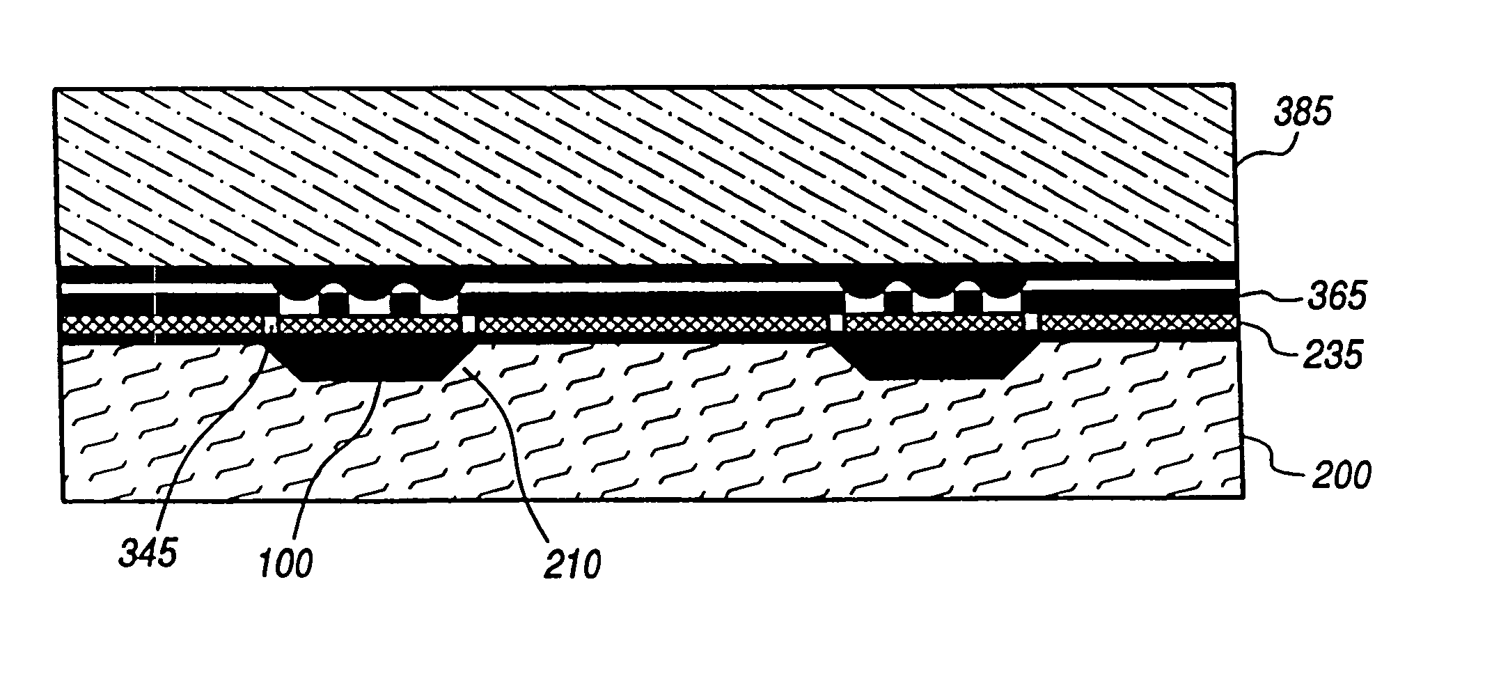
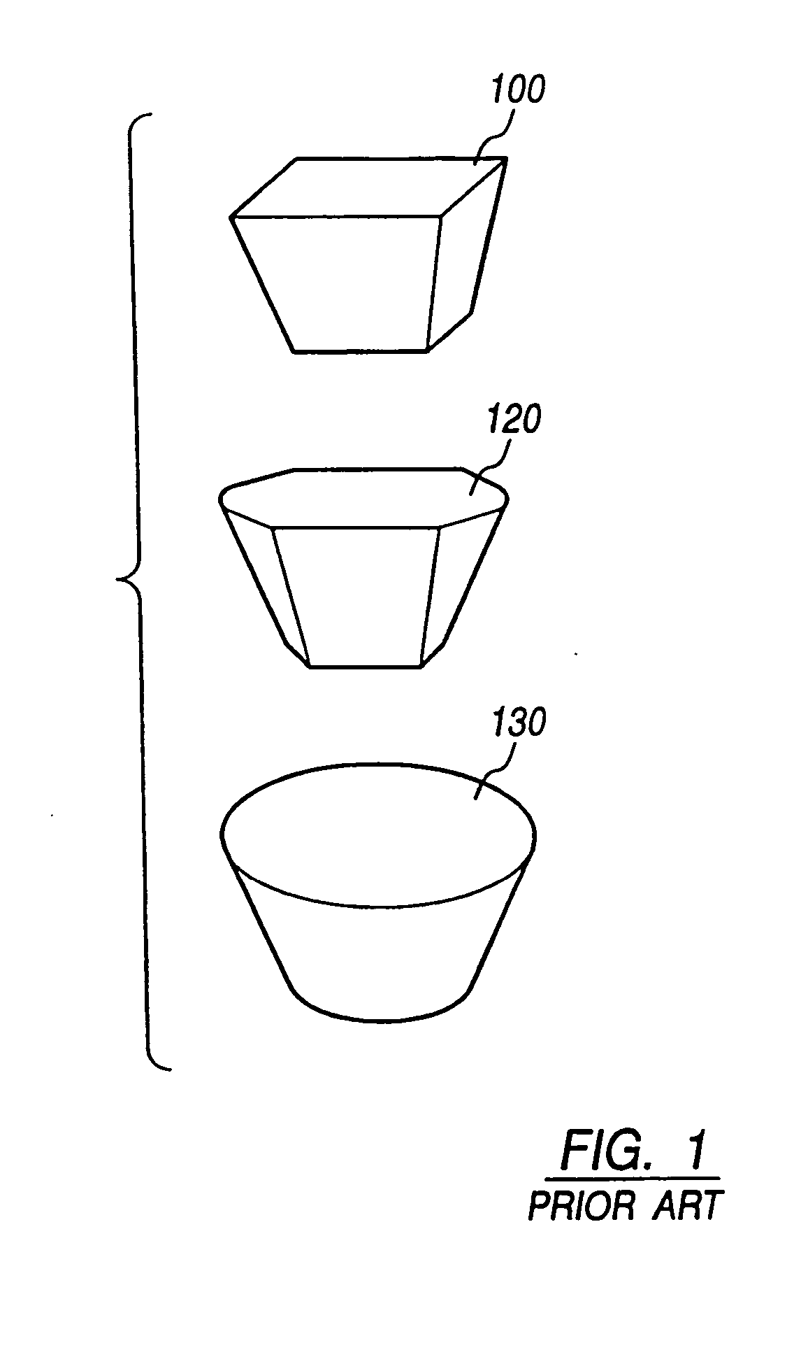
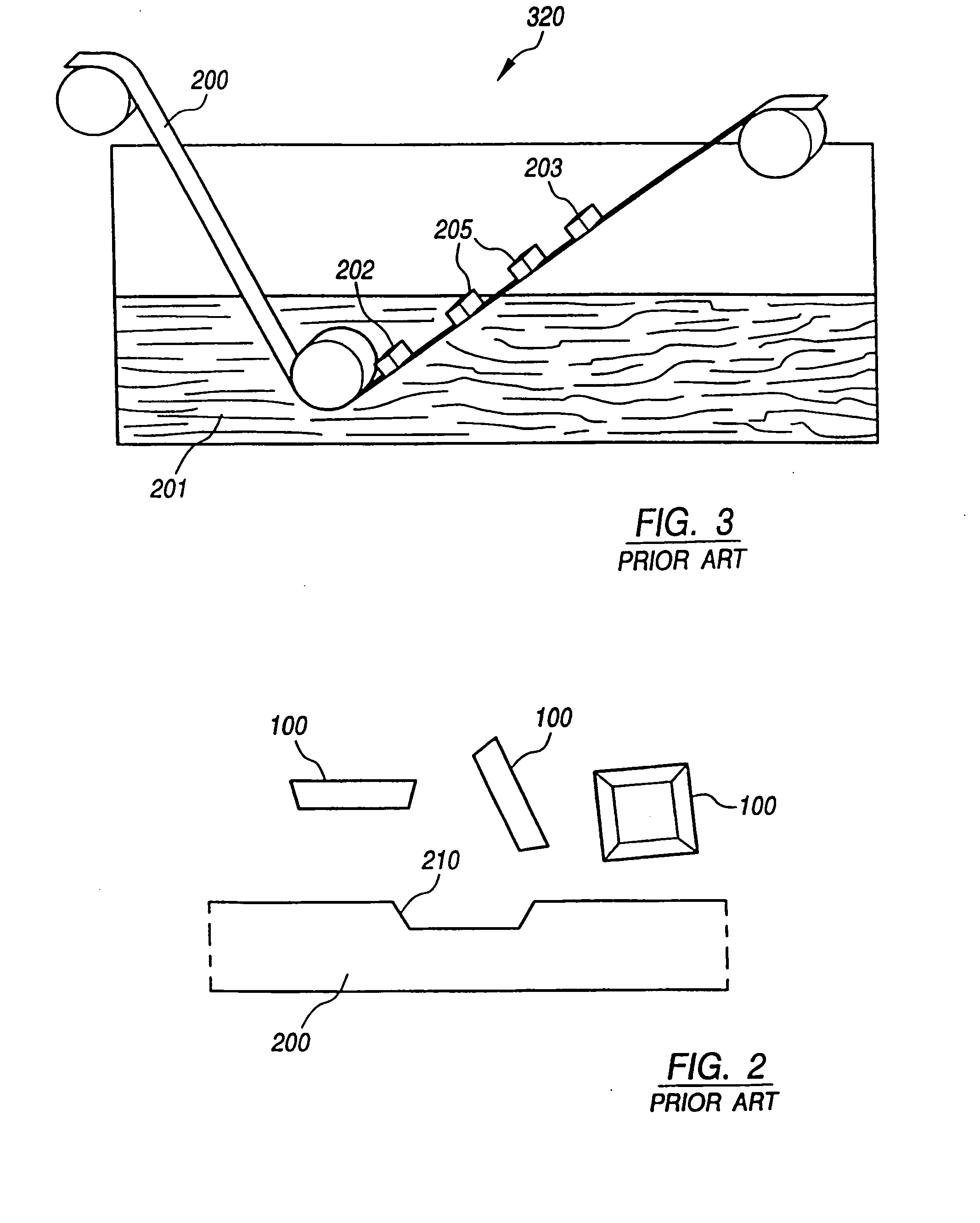
Image

Examples
Embodiment Construction
[0060] There literally are thousands of thermoplastic materials available which may be considered as possible contenders for a substrate that could be formed to provide the necessary shaped receptor microstructure recesses. However, not all can be embossed on a continuous basis; nor can all meet the major general parameters discussed hereinabove or the specifications set forth hereinafter. In accordance with the instant invention, applicants herein have conceived a relationship of parameters defining a rheological window which, when coupled with other specifications, facilitates the identification of materials that will meet the general specifications set forth herein.
[0061] Embossing equipment of the type illustrated in FIG. 14 herein has been used for microreplication of cube corner sheeting and other structures, but typically the embosser runs at lower temperatures. The typical materials used to emboss cube corner sheeting (manufactured, for example using applicants' assignees e...
PUM
 Abstract
Description
Claims
Application Information