Thin-film photoelectric conversion device and a method of manufacturing the same

a technology of conversion device and thin film, which is applied in the direction of sustainable manufacturing/processing, semiconductor devices, climate sustainability, etc., can solve the problems of limited use, low conversion efficiency, limited usable materials, etc., and achieve excellent characteristics of thin film solar cells and the increase of the life of carriers in the crystalline silicon film

Inactive Publication Date: 2006-09-28
SEMICON ENERGY LAB CO LTD
View PDF97 Cites 20 Cited by
  • Summary
  • Abstract
  • Description
  • Claims
  • Application Information

AI Technical Summary

Benefits of technology

[0025] According to the present invention, the lifetime of carriers in the crystalline silicon film is increased, and the excellent characteristics of the thin-film solar cell are obtained.

Problems solved by technology

However, since the amorphous silicon solar cell is lower in conversion efficiency compared with the monocrystal silicon or polycrystal silicon solar cell and also suffers from problems such as deterioration due to light exposure and so on, the use thereof is limited.
In any event, the substrate is required to withstand the crystallization temperature, whereby usable materials are limited.
In particular, in the melt recrystallization method, the substrate has been limited to a material that withstands 1,412° C., which is the melting point of silicon.
However, the amorphous silicon film is hardly crystallized at a temperature of 500° C. or lower.
However, from the viewpoint of reducing the costs of the solar cell, those substrates are not always proper, and it has been desired that the solar cell be fabricated on a substrate which is most generally used and inexpensive.
Also, since a substrate made of a material essentially different from silicon is used, monocrystal cannot be obtained even through crystallization is conducted on the amorphous silicon film through the above means, and silicon having large crystal grains is hard to obtain.
Consequently, this causes a limit to an improvement in the efficiency of the solar cell.
However, since the catalyst materials used for accelerating crystallization are naturally undesirable for crystalline silicon, it has been desired that the concentration of the catalyst material is as low as possible.
However, even when the concentration is relatively low, since the above catalyst materials are heavy metal elements, the material contained in silicon forms a defect level, thereby lowering the characteristics of a fabricated element.
However, when the defect levels are high in silicon, the charges are trapped by the defect levels while they are moving in the silicon, thereby disappearing.

Method used


Image

  • Thin-film photoelectric conversion device and a method of manufacturing the same
  • Thin-film photoelectric conversion device and a method of manufacturing the same
  • Thin-film photoelectric conversion device and a method of manufacturing the same

Examples


first embodiment

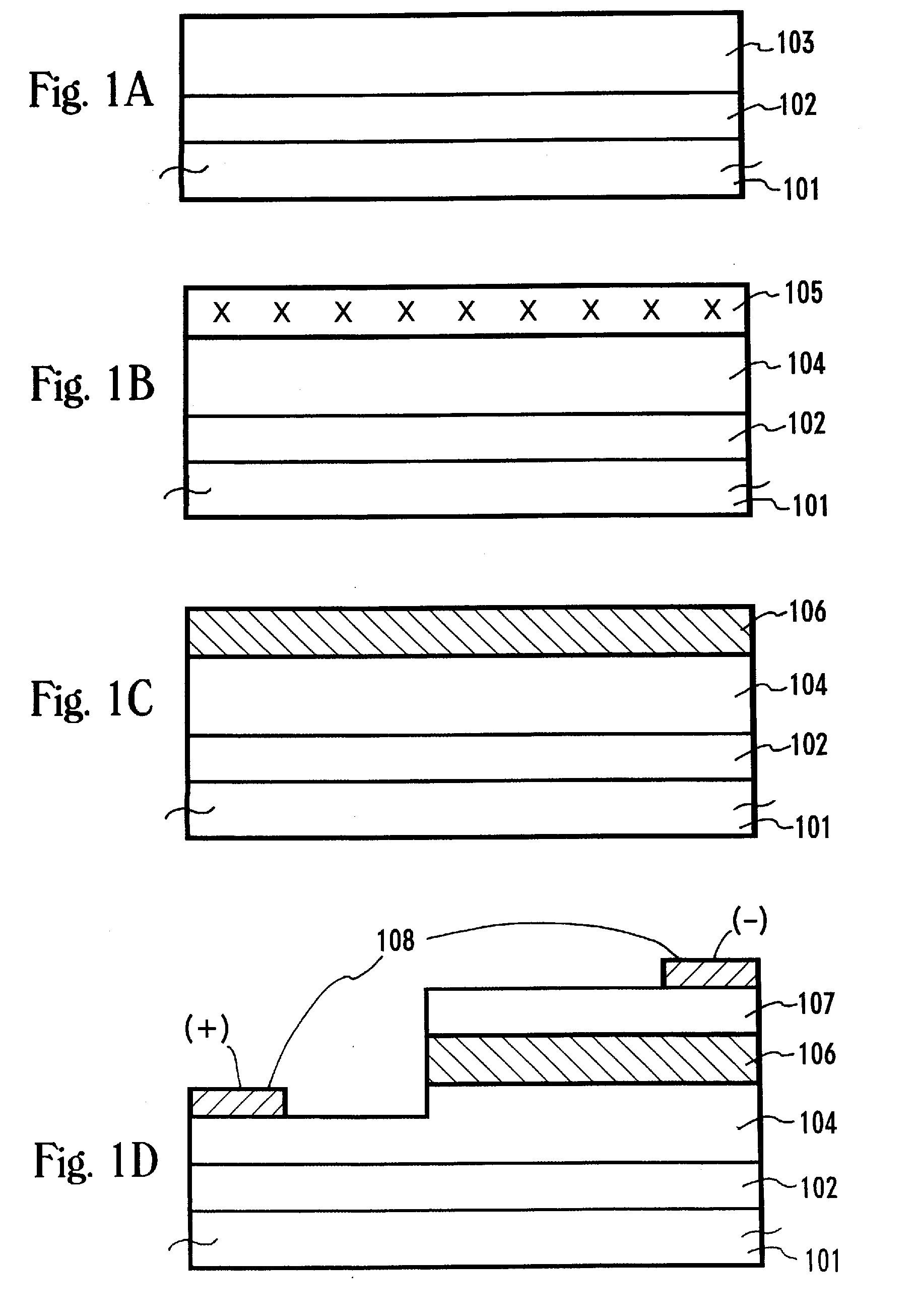
[0032] The first embodiment shows a process of manufacturing a thin-film solar cell through a method of forming an amorphous silicon film in close contact with a metal element that accelerates the crystallization of silicon, crystallizing said amorphous silicon film through a heat treatment, and removing said metal element remaining in the amorphous silicon film after the crystallization.

[0033] This embodiment will be described with reference to FIGS. 1A to 1D. In this embodiment, nickel is used as a metal element having a catalyst action that accelerates the crystallization of silicon. First, a silicon oxide film 102 having a thickness of 0.3 μm is formed on a glass substrate (for example, Corning 7059 glass substrate) 101 as an underlying layer. The silicon oxide film 102 is formed through a plasma CVD technique using tetra ethoxy silane (TEOS as a raw material), and also can be formed through a sputtering technique as another method. Subsequently, an amorphous silicon film 103 i...

second embodiment

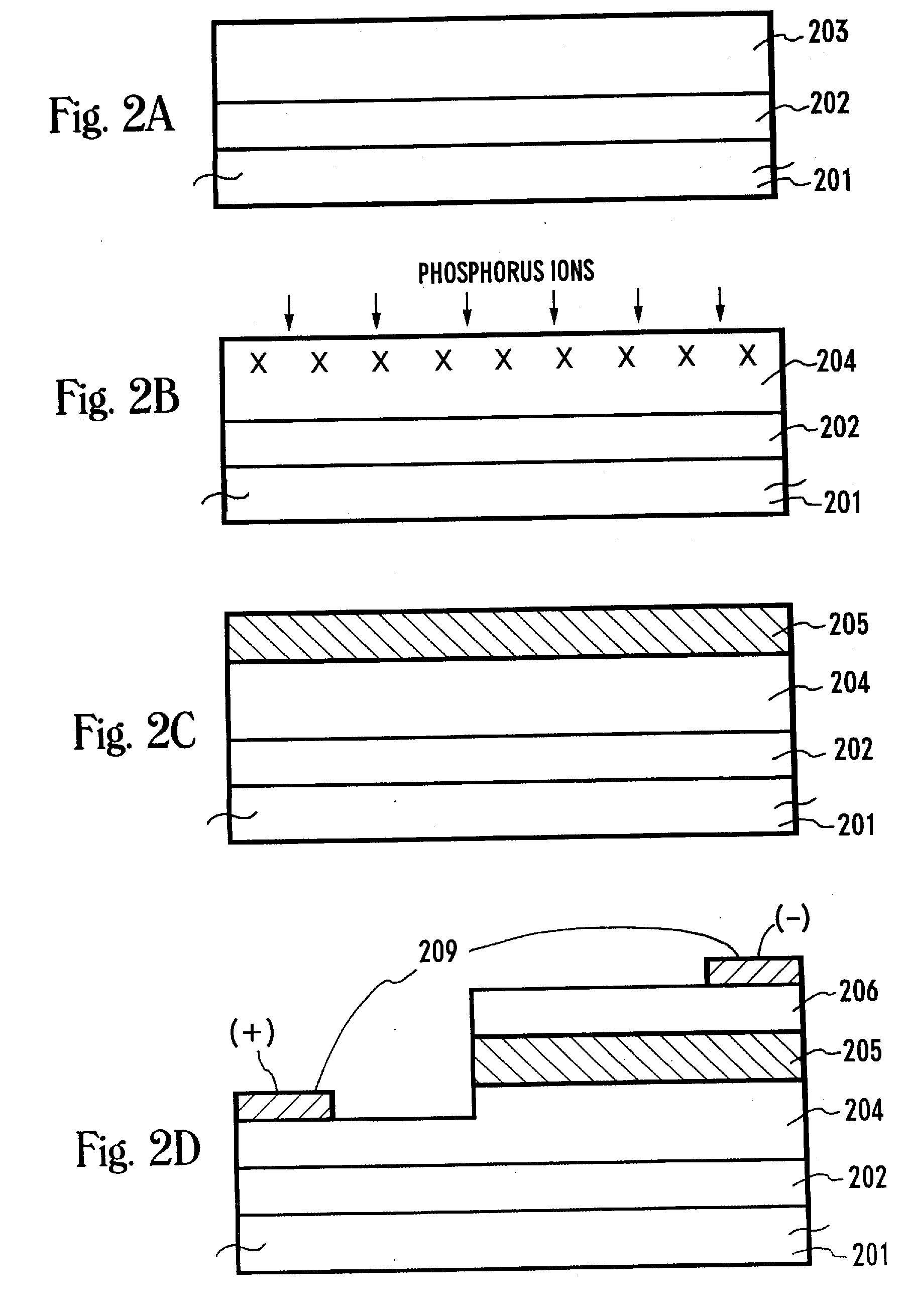
[0040] In a second embodiment, there is described a thin-film solar cell which is formed in a process where a metal element that accelerates the crystallization of crystalline silicon is removed after crystallization, through a method where phosphorus is implanted into the surface of the crystalline silicon film via a plasma doping method.

[0041] The second embodiment will be described with reference to FIGS. 2A to 2D. Nickel is used in this embodiment as a metal element functioning as a catalyst to accelerate the crystallization to accellerate the crystallization of silicon. First, a silicon oxide film 202 having a thickness of 0.3 μm is formed on a glass substrate (for example, Corning 7059 glass substrate) 201 as an underlying layer. The silicon oxide film 202 is formed by plasma CVD with tetra ethoxy silane (TEOS as a raw material), and also can be formed through a sputtering technique as another method. Subsequently, an amorphous silicon film 203 is formed with silane gas as a ...

third embodiment

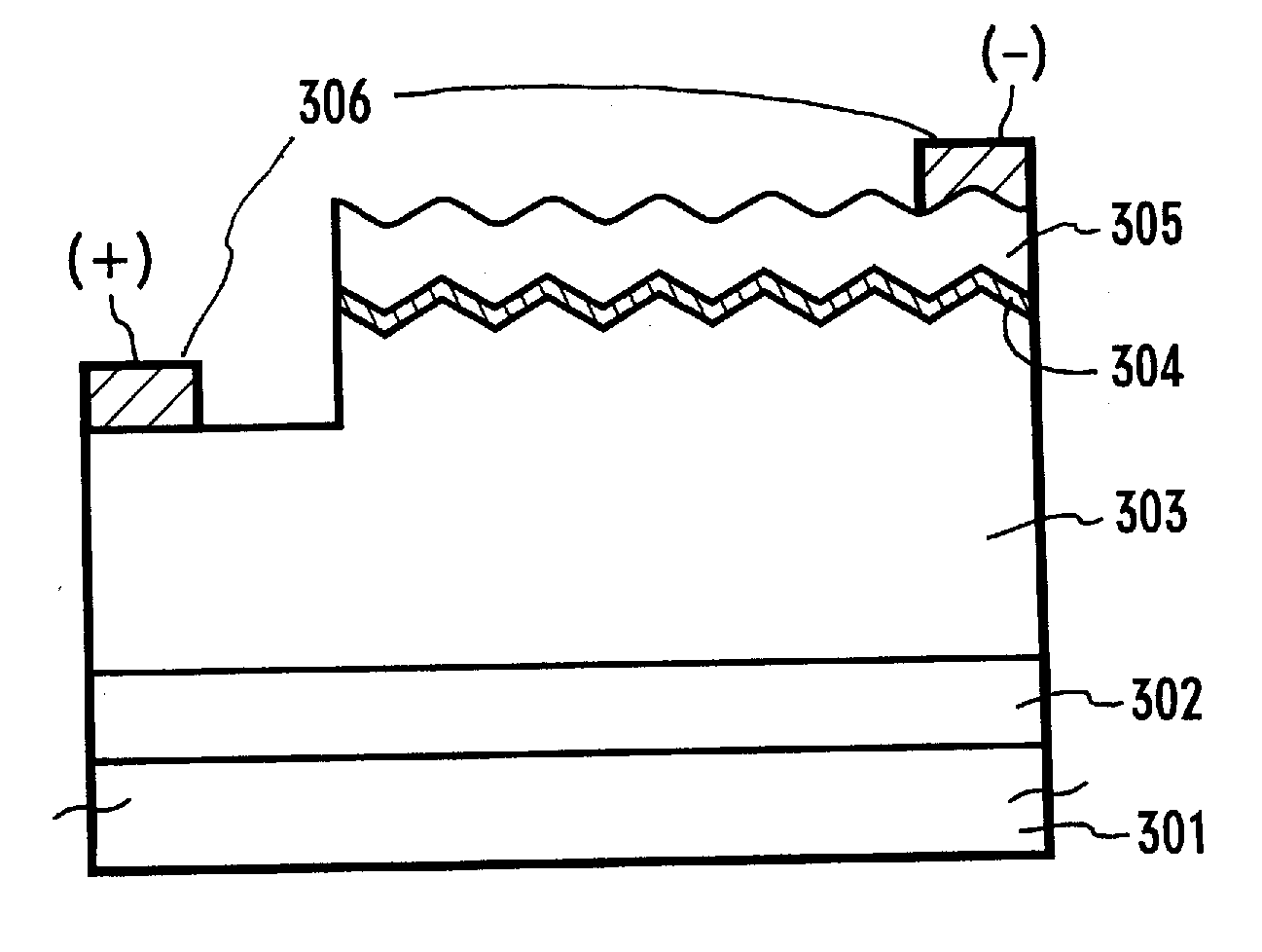
[0049] A third embodiment shows an example where in the process of manufacturing the thin-film solar cell described with reference to the first and second embodiments, the surface of the crystalline silicon film is subjected to an anisotropic etching process so as to make the surface of the solar cell irregular as shown in FIG. 3. A technique by which that surface is made irregular so that reflection from the surface of the solar cell is reduced is called a “texture technique”.

[0050] A silicon oxide film 302 having a thickness of 0.3 μm is formed on a glass substrate (for example, Corning 7059 glass substrate) 301 as an underlying layer. The silicon oxide film 302 is formed by plasma CVD with tetra ethoxy silane (TEOS as a raw material), and also can be formed by sputtering as another method. Subsequently, an amorphous silicon film is formed by plasma CVD. The formation of the amorphous silicon film may be conducted by low pressure thermal CVD, sputtering, evaporation, or the like....


PUM

PropertyMeasurementUnit
melting pointaaaaaaaaaa
temperatureaaaaaaaaaa
strain pointaaaaaaaaaa

Abstract

A method of manufacturing a thin-film solar cell, comprising the steps of: forming an amorphous silicon film on a substrate; placing a metal element that accelerates the crystallization of silicon in contact with the surface of the amorphous silicon film; subjecting the amorphous silicon film to a heat treatment to obtain a crystalline silicon film; depositing a silicon film to which phosphorus has been added in contact with the crystalline silicon film; and subjecting the crystalline silicon film and the silicon film to which phosphorus has been added to a heat treatment to getter the metal element from the crystalline film.

Description

BACKGROUND OF THE INVENTION [0001] 1. Field of the Invention [0002] The present invention relates to a thin-film photoelectric conversion device, especially a solar cell which is formed on a substrate, and more particularly to a thin-film solar cell having a photoelectric conversion layer formed of a crystalline silicon film. [0003] 2. Description of the Related Art [0004] A solar cell or a solar battery can be manufactured using a variety of semiconductor materials or organic compound materials. However, from an industrial viewpoint, silicon is mainly used for the solar cell. The solar cells using silicon can be classified into a bulk solar cell using a wafer of monocrystal silicon or polycrystal silicon and a thin-film solar cell having a silicon film formed on a substrate. Reduction of manufacturing costs is required, and the thin-film solar cell is expected to have the effect of reducing the costs because less raw materials are used for the thin-film solar cell than for the bulk...

Claims


Application Information

Patent Timeline
Patent Type & Authority Applications(United States)
IPC IPC(8): H01L31/00H01L31/068H01L31/18
CPCH01L31/068H01L31/1804Y02E10/547H01L31/1872H01L31/186H01L31/02363H01L31/0682H01L31/022441Y02P70/50H01L31/022425
Inventor YAMAZAKI, SHUNPEIARAI, YASUYUKI
Owner SEMICON ENERGY LAB CO LTD
Why Eureka
Try Eureka