Liquid crystal panel and method of manufacturing the same

a technology of liquid crystal panels and liquid crystals, applied in non-linear optics, instruments, optics, etc., can solve the problems of affecting the filling of liquid crystal, faulty display of liquid crystal panels, and difficulty in liquid crystal filling, so as to prevent air bubbles and effectively maintain cell gaps

Inactive Publication Date: 2006-09-28
SHARP KK
View PDF15 Cites 11 Cited by
  • Summary
  • Abstract
  • Description
  • Claims
  • Application Information

AI Technical Summary

Benefits of technology

[0012] The present invention has been made in view of the above described points, and an object thereof is to provide a liquid crystal panel capable of effectively maintaining a cell gap between a

Problems solved by technology

It is difficult for the liquid crystal filled between the recess and the CF substrate to enter the recesses.
As a consequence, some of these recesses are left behind as vacuum areas, or gasses in the recesses are moved to the liquid crystal layer to thereby cause faulty display of the liquid crystal panel.
However, if small and deep contact holes as described above exist, the air bubbles can remain in the recesses, whereby faulty display of the liquid crystal panel can be caused.
However, to fill recesses remaining at the locations of contact holes after formation of pixel electrodes in the contact holes, with an insulating film, it is necessary to provide a photolithography step of forming the insulating film, and further a flatting step of flatting the formed insulating film, which causes increases in the number of steps and costs.
Further, if columnar spacers for maintaining the cell gap are formed in recesses existing in a

Method used


Image

  • Liquid crystal panel and method of manufacturing the same
  • Liquid crystal panel and method of manufacturing the same
  • Liquid crystal panel and method of manufacturing the same

Examples


first embodiment

[0028] First, a description will be given of a

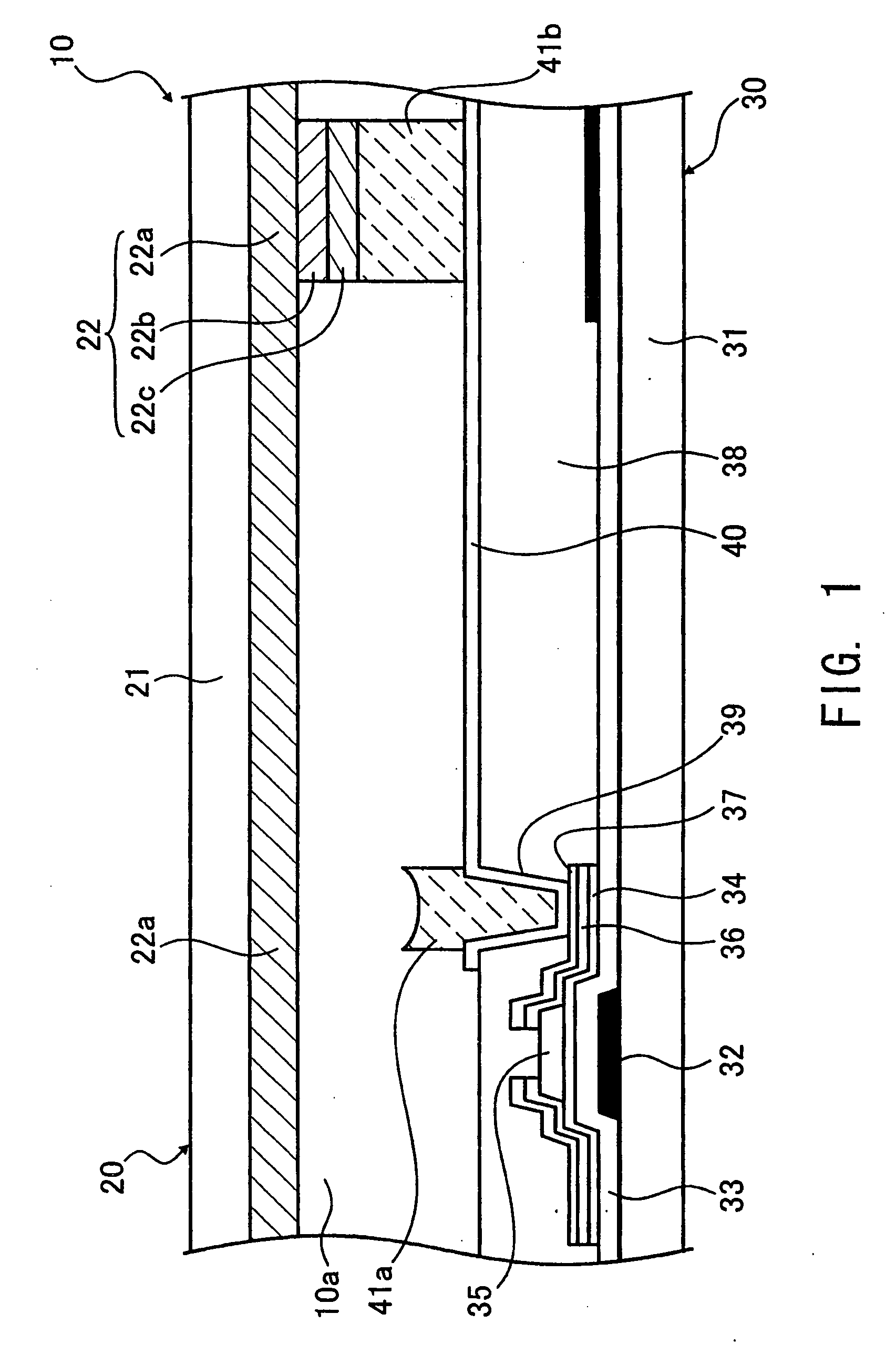
[0029]FIG. 1 is a cross-sectional view of essential elements of a liquid crystal panel according to the first embodiment. It should be noted that FIG. 1 shows only part of the liquid crystal panel, corresponding to one pixel.

[0030] The liquid crystal panel 10 according to the first embodiment includes a CF (Color Filter) substrate 20 and a TFT (Thin Film Transistor) substrate 30 disposed in a manner opposed to each other. Sandwiched between the substrates 20 and 30 is a liquid crystal layer 10a. Further, polarizing plates, not shown, are bonded to respective outer surfaces of the CF substrate 20 and the TFT substrate 30. Thus, the liquid crystal panel 10 is constructed.

[0031] The CF substrate 20 includes a glass substrate 21 made e.g. of no-alkali glass, and a CF layer 22a made of a resin (red resin) having a red color, a resin (green resin) having a green color, or a resin (blue resin) having a blue color, which is formed on a surface...

second embodiment

[0049] Next, a description will be given of the present invention.

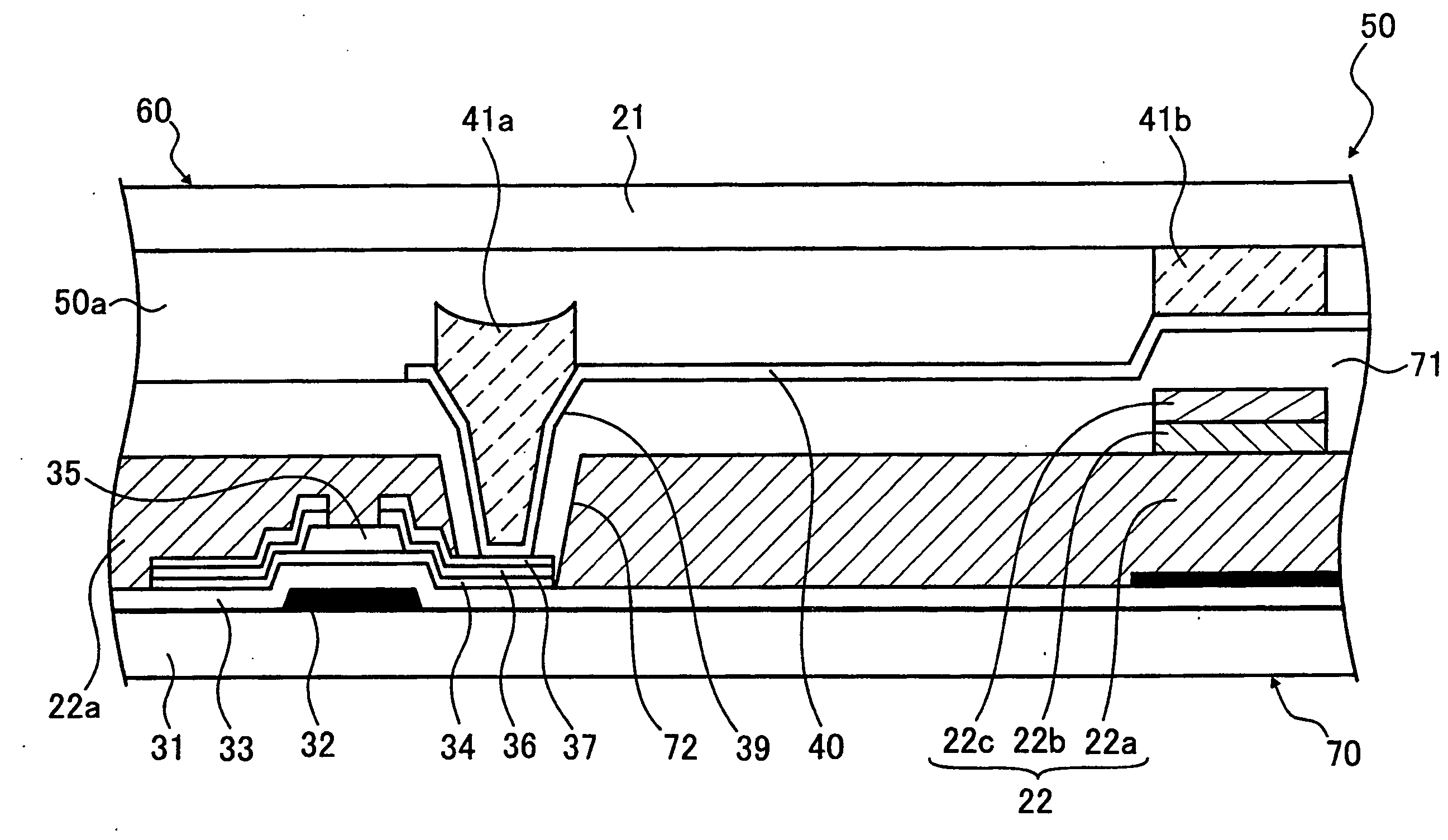
[0050]FIG. 5 is a cross-sectional view of essential elements of a liquid crystal panel according to the second embodiment. It should be noted that FIG. 5 shows only part of the liquid crystal panel, corresponding to one pixel, with component elements identical to those shown in FIG. 1 being designated by identical reference numerals, and detailed description thereof is omitted.

[0051] The liquid crystal panel 50 according to the second embodiment is distinguished from the liquid crystal panel 10 according to the first embodiment in that it has a structure in which a common electrode substrate 60 and a TFT substrate 70 are bonded to each other with a liquid crystal layer 50a sandwiched therebetween, and CF layers 22a, 22b, and 22c are formed on the TFT substrate 70 side.

[0052] The common electrode substrate 60 as a counter substrate opposed to the TFT substrate 70 has a basic structure in which a common electrode, not...

third embodiment

[0057] Next, a description will be given of the present invention.

[0058]FIG. 6 is a cross-sectional view of essential elements of a liquid crystal panel according to the third embodiment. FIG. 7 is a cross-sectional view taken on line A-A of FIG. 6. It should be noted that FIG. 6 and FIG. 7 show only part of the liquid crystal panel, corresponding to one pixel, with component elements identical to those shown in FIG. 5 being designated by identical reference numerals, and detailed description thereof is omitted.

[0059] The liquid crystal panel 80 according to the third embodiment is distinguished from the liquid crystal panel 50 according to the second embodiment in that it has a structure in which a common electrode substrate 60a and a TFT substrate 70a are bonded to each other, with a liquid crystal layer 80a sandwiched therebetween, protrusions 61 of dielectric layers are formed on a common electrode formed on the common electrode substrate 60a, and two slits 73 are formed in a p...


PUM


Abstract

There is provided a liquid crystal panel capable of maintaining a cell gap and preventing generation of air bubbles. In the liquid crystal panel having a liquid crystal layer sandwiched between a color filter (CF) substrate and a thin film transistor (TFT) substrate, recesses formed at respective locations of contact holes each for connecting a drain metal layer and a pixel electrode to each other are filled with respective hole-filling columnar layers. At the same time, the cell gap between the CF substrate and the TFT substrate is maintained by cell gap-maintaining columnar layers. The columnar layers are simultaneously formed by subjecting a photosensitive resin to exposure and development. As a result, a reliable liquid crystal panel which does not suffer from air bubbles remaining in the recesses formed at the locations of the contact holes, and capable of effectively maintaining the cell gap with high productivity at low costs.

Description

[0001] This is a Divisional of application Ser. No. 10 / 806,079, filed Mar. 22, 2004.BACKGROUND OF THE INVENTION [0002] (1) Field of the Invention [0003] This invention relates to a liquid crystal panel and a method of manufacturing the same, and more particularly to a liquid crystal panel having a structure in which recesses formed at respective locations of contact holes each for making contact between a pixel electrode on a TFT (Thin Film Transistor) substrate and a TFT are filled with a resin or the like, and a method of manufacturing the same. [0004] (2) Description of the Related Art [0005] A liquid crystal panel mounted in a liquid crystal display device has a structure in which a liquid crystal layer is sandwiched between a TFT substrate mainly formed with pixel electrodes, TFTs for driving pixel electrodes, and bus lines, and a counter substrate, such as a CF substrate, mainly formed with pixel electrodes and color filters (CFs), with polarizing plates bonded to the substrat...

Claims


Application Information

Patent Timeline
IPC IPC(8): G02F1/136G02F1/1335G02F1/1339G02F1/1362G02F1/1368
CPCG02F1/13394G02F1/136227
Inventor TANIGUCHI, YOJINAKAHATA, YUJI
Owner SHARP KK
Why Eureka
Try Eureka