Method and apparatus for detecting pattern defects

a pattern defect and pattern technology, applied in the field of visual inspection methods, can solve the problems of classes, unfavorable classification of features, etc., and achieve the effect of correct setting classification conditions

Inactive Publication Date: 2006-09-28
HITACHI HIGH-TECH CORP
View PDF8 Cites 32 Cited by
  • Summary
  • Abstract
  • Description
  • Claims
  • Application Information

AI Technical Summary

Benefits of technology

[0005] The present invention has been made to solve the above mentioned problem, and an object of the present invention is to provide a visual inspection method, and an apparatus, which are capable of correctly setting classification conditions even if a defect occurrence ratio deviates from the usual.
[0013] According to the present invention, it is possible to equally review and teach defects of each class irrespective of an occurrence ratio of them by performing sampling of defects on the basis of the distribution of defect features. Therefore, it is possible to correctly keep track of the relationship between a defect class and a feature only with a small number of reviews, and thereby to set classification conditions that will produce correct results.

Problems solved by technology

Therefore, because it is practically impossible to review all defects, it is necessary to sample defects, the number of which is from several tens to several hundreds, before the sampled defects are reviewed.
However, when defects are sampled at random, if a defect occurrence ratio deviates from the usual, the same kind of defects are mainly selected, resulting in the unclear relationship between a feature and a class.
Accordingly, classification conditions cannot be correctly set, which was a problem to be solved.

Method used


Image

  • Method and apparatus for detecting pattern defects
  • Method and apparatus for detecting pattern defects
  • Method and apparatus for detecting pattern defects

Examples


first embodiment

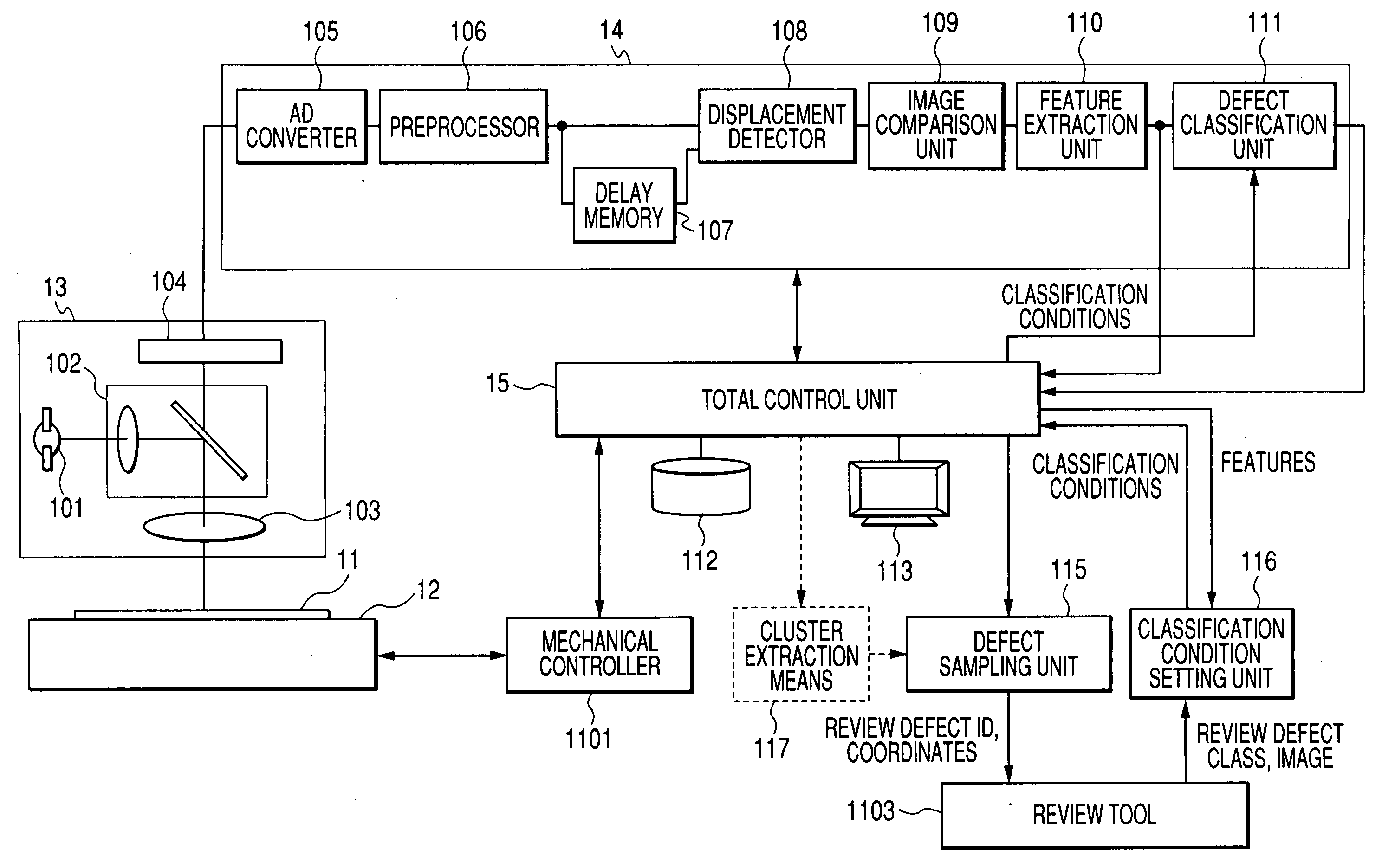
[0028] First of all, a first embodiment of a visual inspection method and an apparatus according to the present invention will be described in detail with reference to FIGS. 1 through 8.

[0029] A first embodiment of an optical visual inspection apparatus targeted for semiconductor wafers will be described. FIG. 1 is a diagram illustrating a configuration of an optical visual inspection apparatus according to the first embodiment of the present invention. The optical visual inspection apparatus is configured to include a stage 12 to place a target substrate 11 such as a semiconductor wafer thereon and to be moved, and a detector 13. The detector 13 comprises: a light source 101 emitted a light beam for irradiating a illumination light beam onto the target substrate 11; an illumination optical system 102 for condensing the light beam emitted from the light source 101; an objective lens 103 for irradiating the target substrate 11 with the illumination light beam condensed by the illumi...

second embodiment

[0066] Next, a second embodiment of a visual inspection method and an apparatus according to the present invention will be described with reference to FIG. 9. A point of difference between the first and second embodiments is that a processing method carried out by the defect sampling unit 115 in the second embodiment differs from that in the first embodiment. In the first embodiment, sections are full automatically and semiautomatically set in the feature space. However, sections are manually set in the second embodiment. This method will be described as below.

[0067] According to an instruction from the user interface 113 after inspection, the defect sampling unit 115 inputs feature data of each defect corresponding to each defect ID that has been extracted and then has been stored in the storage device 112 by the feature extraction unit 110. Next, the defect sampling unit 115 creates a histogram illustrating features of defects, and then displays the histogram on the user interfac...

third embodiment

[0072] Next, a third embodiment of a visual inspection method and an apparatus according to the present invention will be described with reference to FIGS. 10A, 10B, 10C. Paying attention to the third embodiment, a point of difference between the first and second embodiments is that a processing method carried out by the defect sampling unit 115 in the third embodiment differs from that in the first and second embodiments. In the first and second embodiments, sampling is performed on the basis of defect features based on detected image information. However, in the third embodiment, sampling is performed by use of position information of defects in combination with the above-mentioned defect features.

[0073] First of all, a first method in the third embodiment will be described. In the first method, the defect position information used in combination with the defect features is the shortest distance from the adjacent defect, the local defect density and the like, calculated by using,...


PUM


Abstract

With the objective of achieving defect kind training in a short period of time to teach classification conditions of defects detected as a result of inspecting a thin film device, according to one aspect of the present invention, there is provided a visual inspection method, and an apparatus therefor, comprising the steps of: detecting defects based on inspection images acquired by optical or electronic defect detection means, and at the same time calculating features of the defects; and classifying the defects according to classification conditions set beforehand, wherein said classification condition setting step further includes the steps of: collecting defect features over a large number of defects acquired beforehand from the defect detection step; sampling defects based on the distribution of the collected defect features over the large number of defects; and setting defect classification conditions based on the result of reviewing the sampled defects.

Description

BACKGROUND OF THE INVENTION [0001] The present invention relates to a visual inspection method, and an apparatus, for detecting defects including minute pattern defects and particles on the basis of an image of an object, which has been acquired by use of lamp light, a laser beam, an electron beam, or the like, and for classifying the defects, the visual inspection method and apparatus being targeted for thin film devices including a semiconductor wafer, TFT, and a photo mask. In particular, the present invention relates to a visual inspection method and an apparatus that are suitable for visual inspection of a semiconductor wafer. [0002] Thin film devices such as a semiconductor wafer, a liquid crystal display, and a magnetic head of a hard disk are manufactured through many fabrication processes. In the manufacturing of such thin film devices, with the objective of improving and stabilizing yields, visual inspection is performed for each series of processes. In the visual inspecti...

Claims


Application Information

Patent Timeline
Patent Type & Authority Applications(United States)
IPC IPC(8): G06K9/00
CPCG01N21/9501G01N21/95607G01N2021/8854G01N2021/95676G06K9/6221G06F18/2321
Inventor SHIBUYA, HISAEHAMAMATSU, AKIRATAKAGI, YUJI
Owner HITACHI HIGH-TECH CORP
Why Eureka
Try Eureka