

System and method to customize bond programs compensating integrated circuit bonder variability
a technology of integrated circuit bonding and program customization, applied in the field of electronic systems and semiconductor devices, can solve the problems of reducing the accuracy of pattern recognition system reference placement, wire bonding techniques, and the inability of the bond head to place the bonds, so as to reduce the error rate of operation program
- Summary
- Abstract
- Description
- Claims
- Application Information
AI Technical Summary
Benefits of technology
Problems solved by technology
Method used
Image

Examples
Embodiment Construction
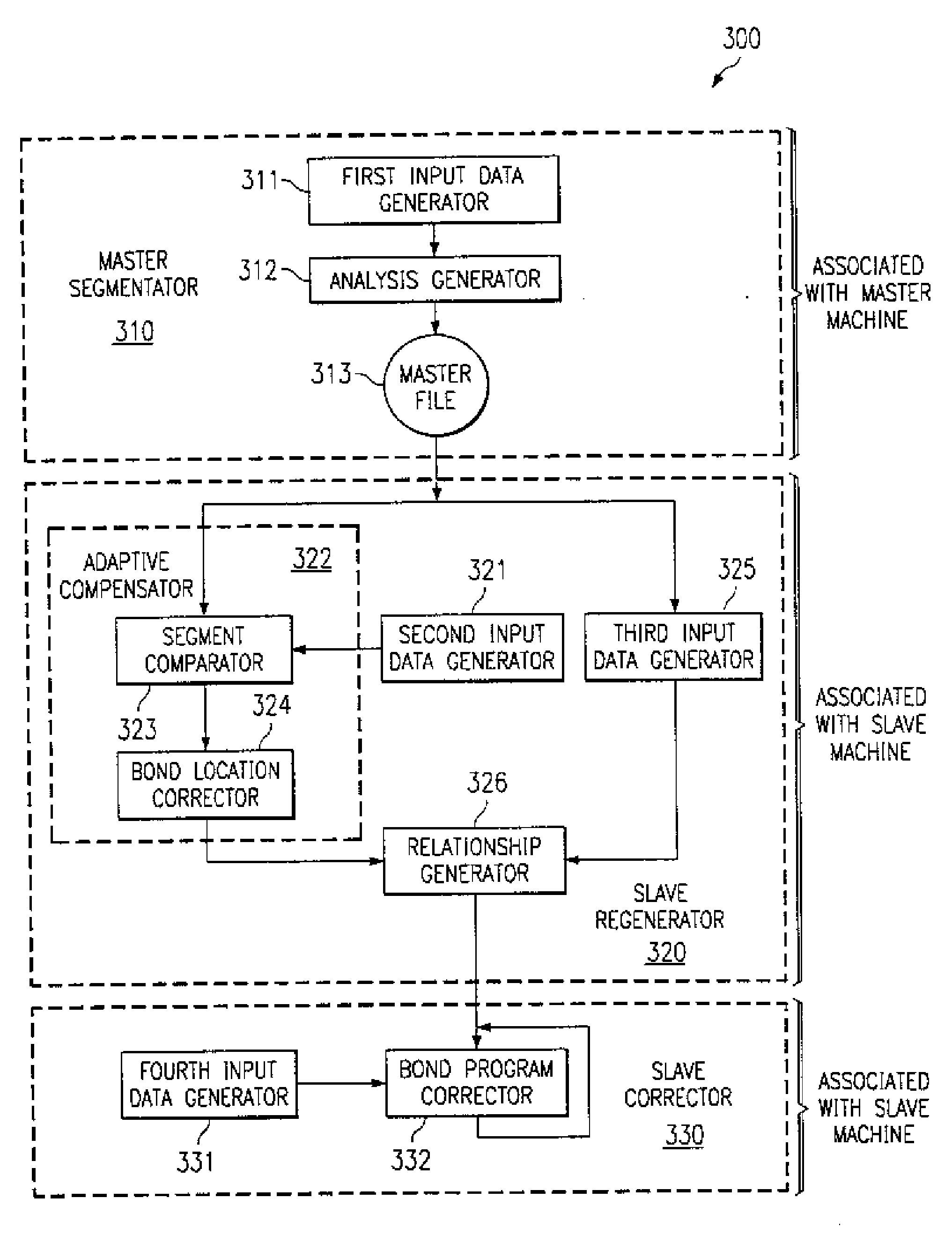
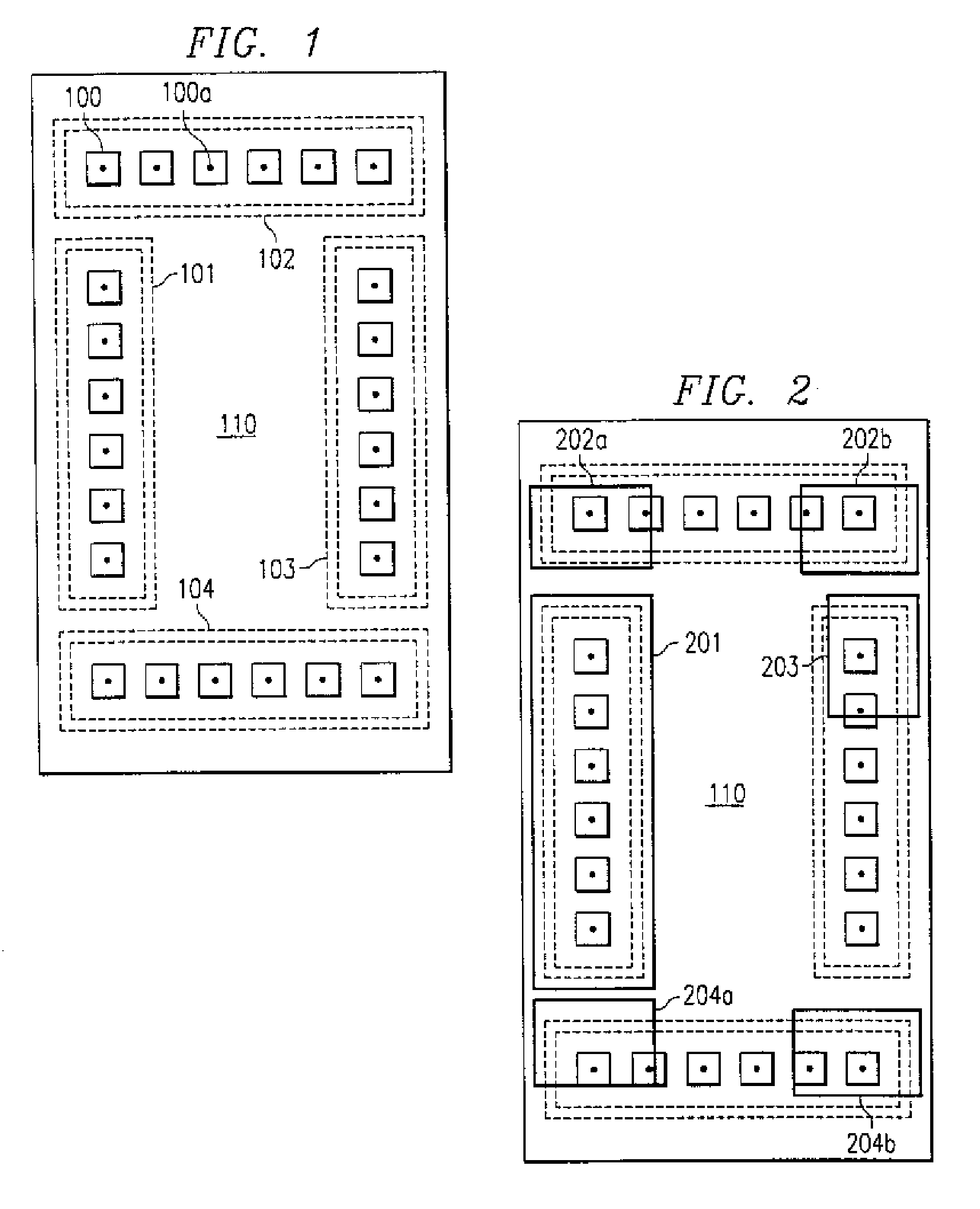
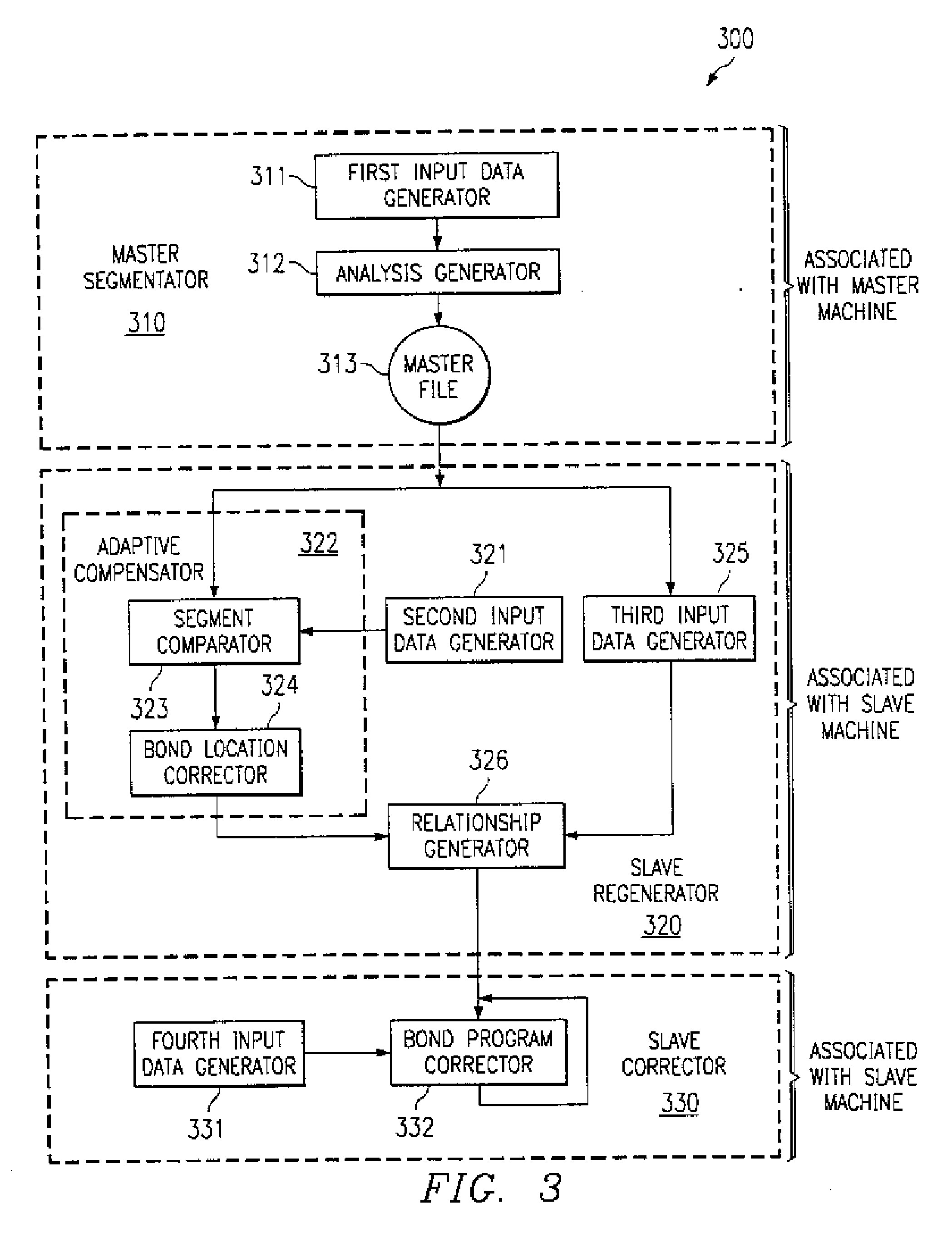
[0046] In order to eliminate variability of the automated bonding machines (“bonders”), which may depend on the specific apparatus or may be time-dependent, the invention uses the approach to group a small set of bond pad locations into “segments” during the device program “teaching”. As examples, FIGS. 1 and 2 illustrate the approach and the solution to problems in assembling semiconductor chip 110 caused by machine-related errors in bonding operation. As illustrated in FIG. 1, a plurality of bond pads 100 lined up along one of the x or y axes may be grouped as a segment. All or some of the bond pads may be grouped into different segments, such as the four segments 101, 102, 103, and 104 in FIG. 1, each containing six bond pads. Within the small stretch covered by the segment, it may be assumed that the bonding tables behave linearly (polynomially). (In the ideal assembly case illustrated, all bonds 100a attached to pads 100 are located in the center of the pad areas.)
[0047] Each ...
PUM
 Abstract
Description
Claims
Application Information