CMOS SRAM cells employing multiple-gate transistors and methods fabricating the same

Inactive Publication Date: 2006-10-05
SAMSUNG ELECTRONICS CO LTD
View PDF16 Cites 88 Cited by
  • Summary
  • Abstract
  • Description
  • Claims
  • Application Information

AI Technical Summary

Benefits of technology

[0011] Still further embodiments of the present invention include met

Problems solved by technology

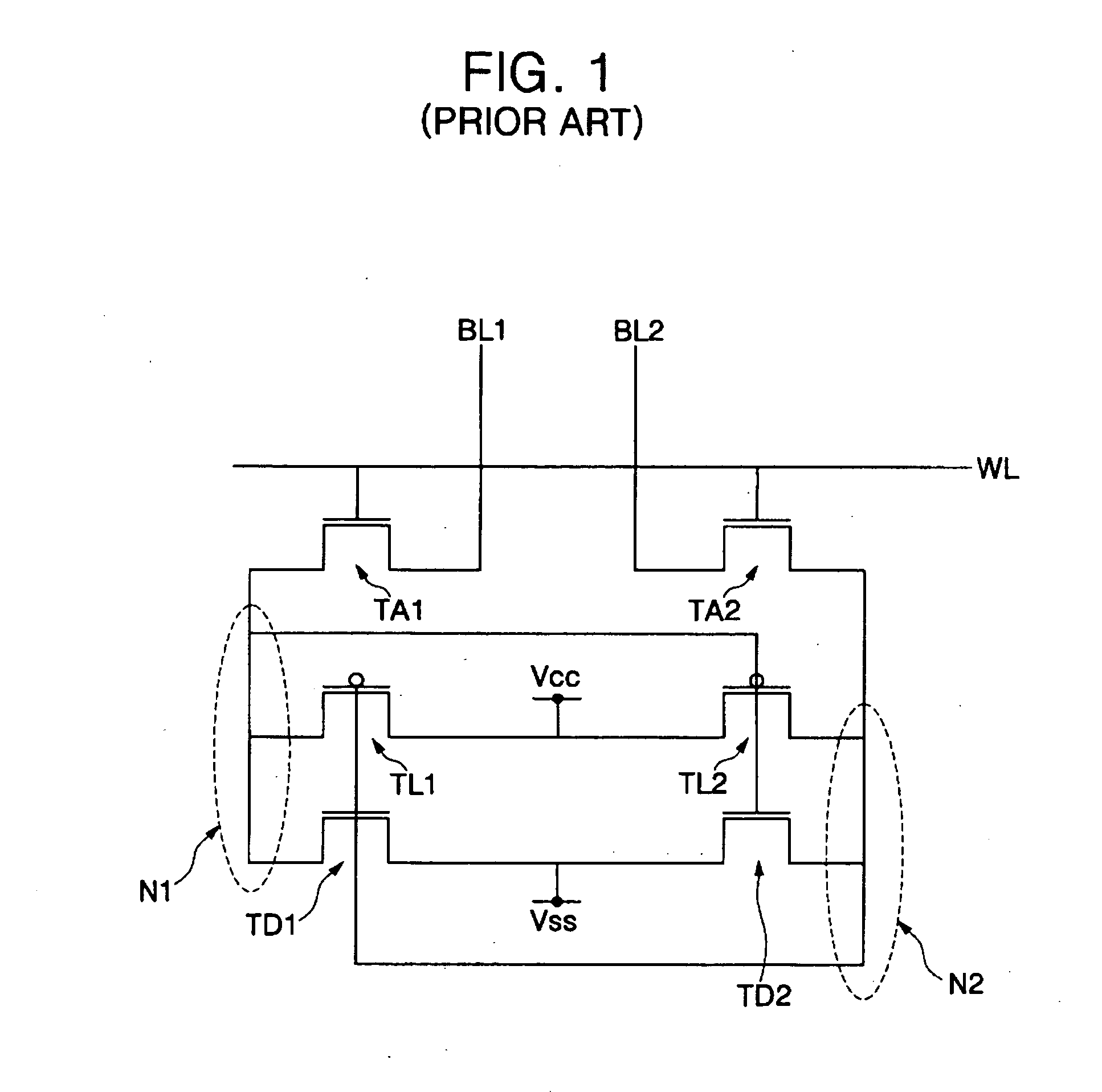
However, the bulk CMOS SRAM cell has a relatively lo

Method used


Image

  • CMOS SRAM cells employing multiple-gate transistors and methods fabricating the same
  • CMOS SRAM cells employing multiple-gate transistors and methods fabricating the same
  • CMOS SRAM cells employing multiple-gate transistors and methods fabricating the same

Examples


Embodiment Construction

[0020] The present invention will now be described more fully hereinafter with reference to the accompanying drawings, in which exemplary embodiments of the invention are shown. This invention may, however, be embodied in different forms and should not be construed as limited to the embodiments set forth herein. Rather, these embodiments are provided so that this disclosure will be thorough and complete, and will fully convey the scope of the invention to those skilled in the art. In the drawings, the thickness of layers and regions are exaggerated for clarity. In addition, when a layer is described to be formed on other layer or on a substrate, which means that the layer may be formed on the other layer or on the substrate, or a third layer may be interposed between the layer and the other layer or the substrate. Like numbers refer to like elements throughout the specification.

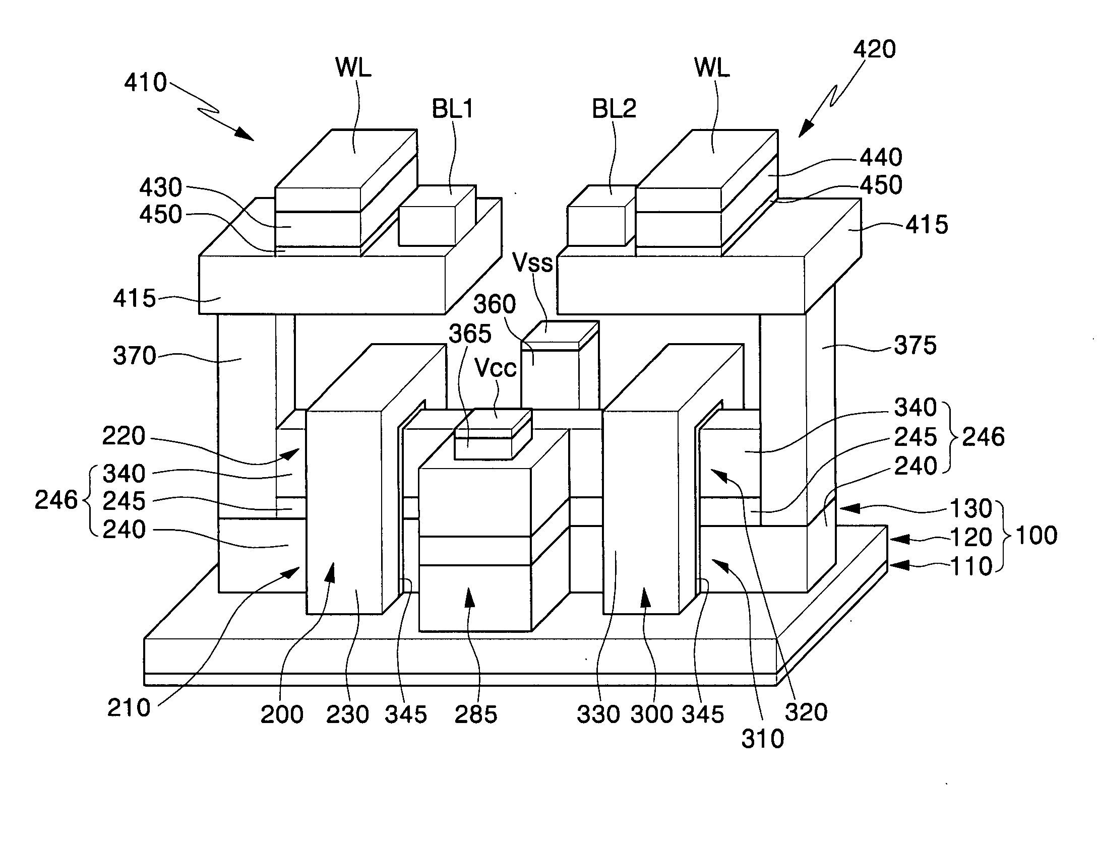
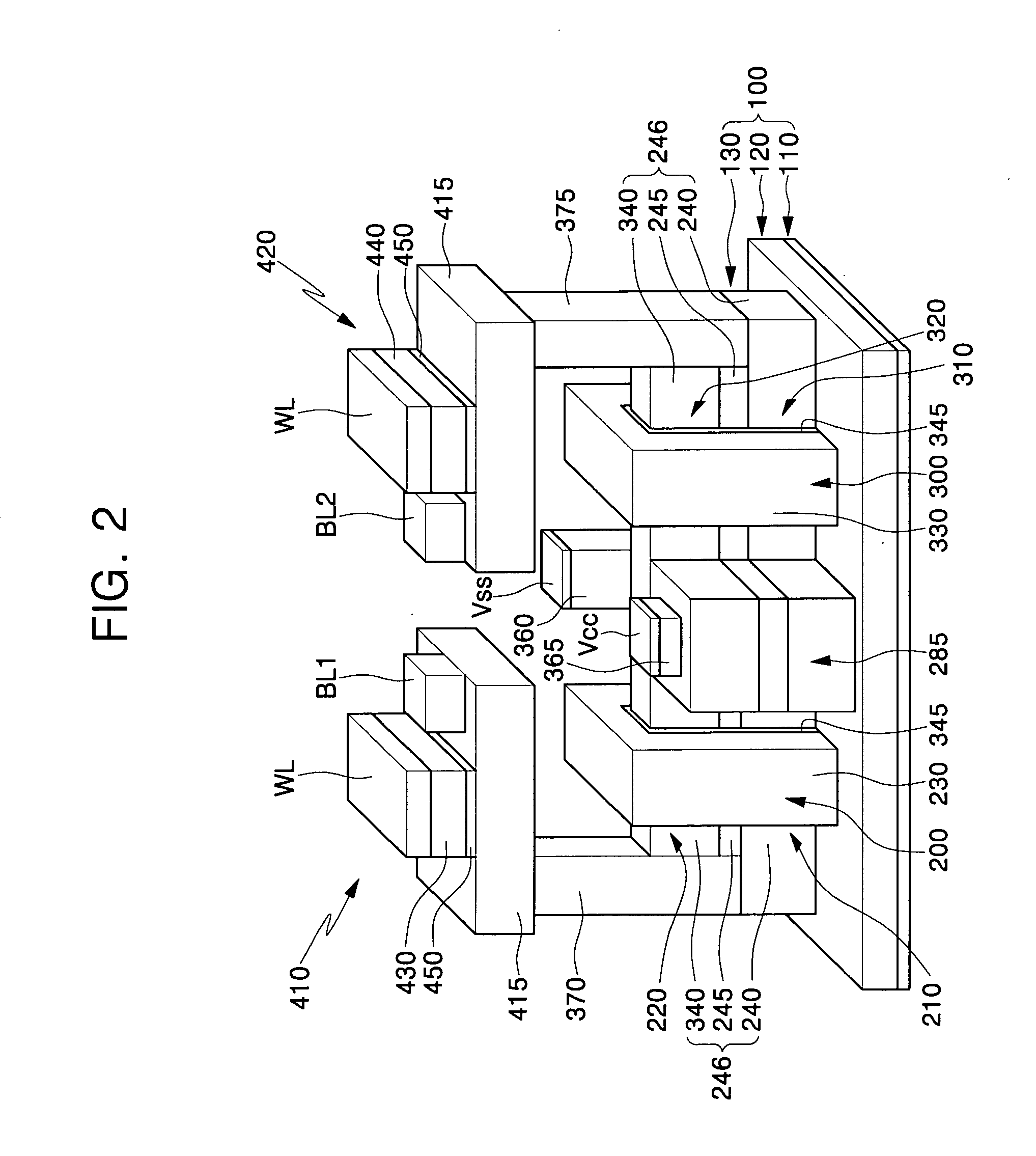
[0021] Referring to FIGS. 2 and 3A, a CMOS SRAM cell according to an embodiment of the present invention ...


PUM

PropertyMeasurementUnit
Electrical conductivityaaaaaaaaaa
Semiconductor propertiesaaaaaaaaaa

Abstract

Complementary metal oxide semiconductor (CMOS) static random access memory (SRAM) cells include at least a first inverter formed in a fin-shaped pattern of stacked semiconductor regions of opposite conductivity type. In some of these embodiments, the first inverter includes a first conductivity type (e.g., P-type or N-type) MOS load transistor electrically coupled in series with a second conductivity type (e.g., N-type of P-type) MOS driver transistor. The first inverter is arranged so that active regions of the first conductivity type MOS load transistor and the second conductivity type driver transistor are vertically stacked relative to each other within a first portion of a vertical dual-conductivity semiconductor fin structure. This fin structure is surrounded on at least three sides by a wraparound gate electrode, which is configured to modulate conductivity of both the active regions in response to a gate signal.

Description

REFERENCE TO PRIORITY APPLICATION [0001] This application claims the benefit of Korean Patent Application No. 2005-21996, filed Mar. 16, 2005, the disclosure of which is hereby incorporated herein by reference. FIELD OF THE INVENTION [0002] The present invention relates to semiconductor memory devices and methods of fabricating the same and, more particularly, to complementary metal oxide semiconductor static random access memory (CMOS SRAM) cells and methods of fabricating the same. BACKGROUND OF THE INVENTION [0003] A static random access memory (SRAM) has the advantages of low power consumption and fast operating speed compared to a dynamic RAM (DRAM). Accordingly, the SRAM is widely employed in a portable appliance or a cache memory device of a computer. A unit cell of the SRAM is mainly classified into two types. One of them is a high load resistor SRAM cell, which employs a high load resistor as a load device, and the other is a CMOS SRAM cell, which employs a P-channel MOS (P...

Claims


Application Information

Patent Timeline
IPC IPC(8): H01L27/12
CPCH01L21/84H01L27/11H01L29/785H01L27/1108H01L27/1203H01L27/1104Y02E20/32H10B10/00H10B10/125H10B10/12B01D53/1475B01D53/1412B01D53/96F16K1/22F16K27/0218F23J15/02B01D2257/504B01D2251/304B01D2251/306B01D2251/606Y02C20/40
Inventor HUO, ZONG-LIANGBAIK, SEUNG-JAEYEO, IN-SEOKYOON, HONG-SIKKIM, SHI-EUN
Owner SAMSUNG ELECTRONICS CO LTD
Why Eureka
Try Eureka