Boundary scan controller, semiconductor device, method for identifying semiconductor circuit chip of semiconductor device, and method for controlling semiconductor circuit chip of semiconductor device

a scan controller and semiconductor technology, applied in the direction of solid-state devices, pulse techniques, instruments, etc., can solve the problem that the same chips cannot be stacked

Inactive Publication Date: 2006-10-05
SHARP KK
View PDF14 Cites 16 Cited by
  • Summary
  • Abstract
  • Description
  • Claims
  • Application Information

AI Technical Summary

Benefits of technology

[0028] An object of the present invention is to provide a boundary scan controller which can perform a boundary sc...

Problems solved by technology

In the case of performing the boundary scans, it is only the chip assembly of the uppermost stage that needs to be made the separate chip assembly, as elucidated in FIGS. 17 and 18, but in a case where th...

Method used


Image

  • Boundary scan controller, semiconductor device, method for identifying semiconductor circuit chip of semiconductor device, and method for controlling semiconductor circuit chip of semiconductor device
  • Boundary scan controller, semiconductor device, method for identifying semiconductor circuit chip of semiconductor device, and method for controlling semiconductor circuit chip of semiconductor device
  • Boundary scan controller, semiconductor device, method for identifying semiconductor circuit chip of semiconductor device, and method for controlling semiconductor circuit chip of semiconductor device

Examples


Embodiment Construction

[0092] Now referring to the drawings, preferred embodiments of the invention are described below.

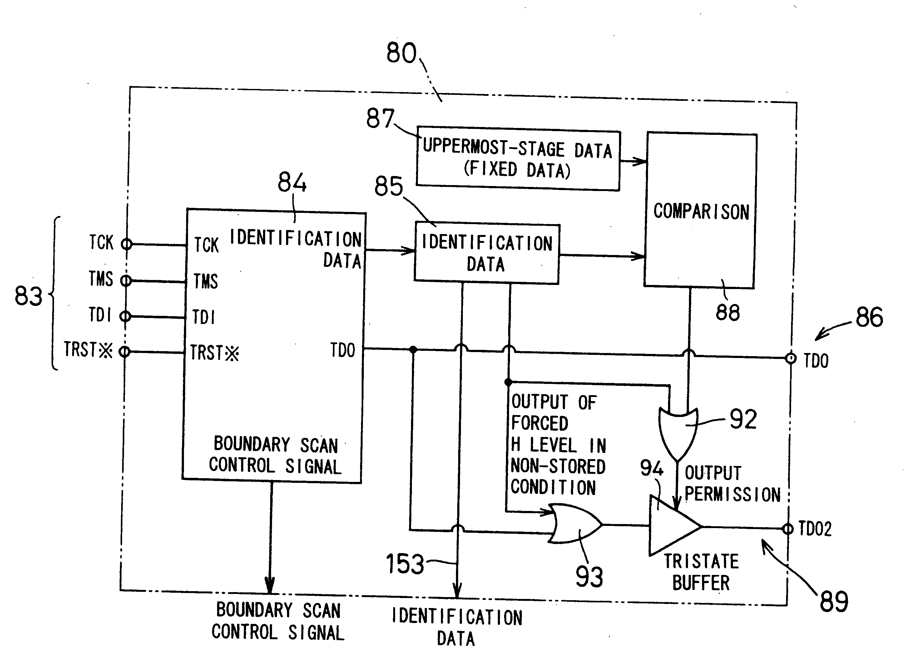
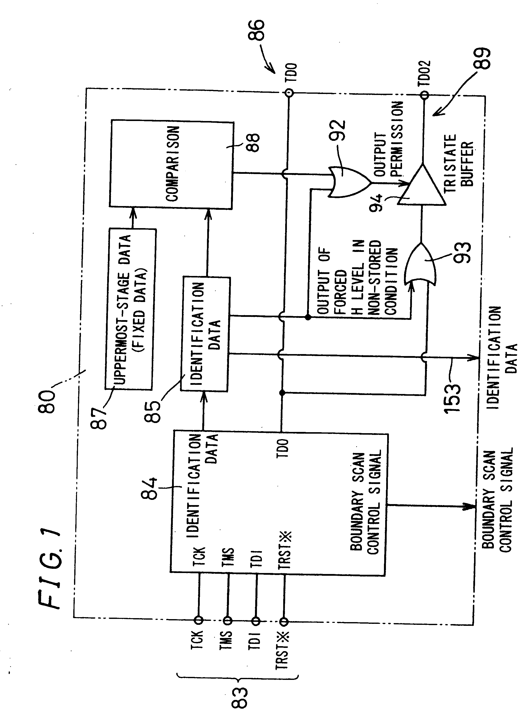
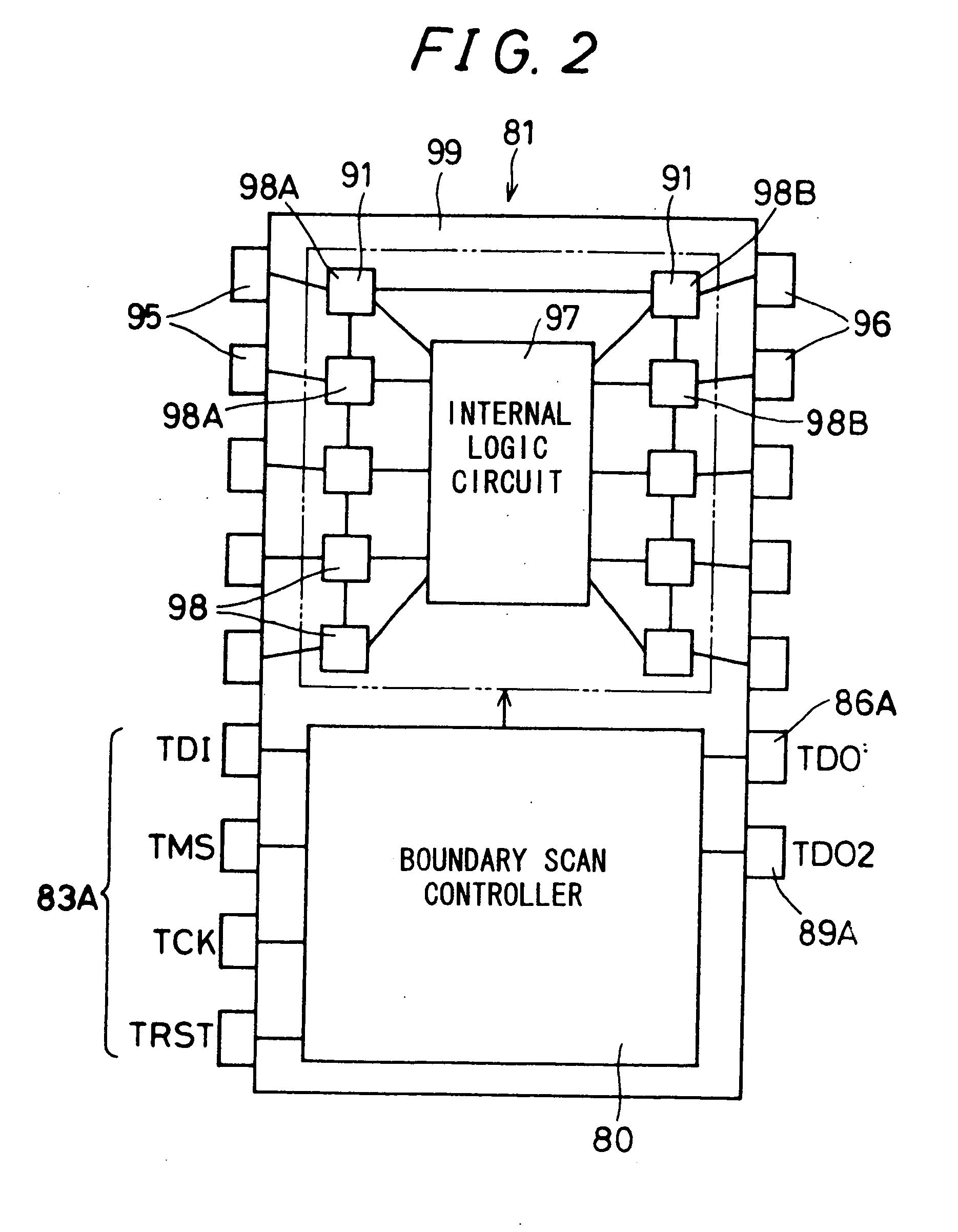
[0093]FIG. 1 is a block diagram showing a boundary scan controller 80 according to one embodiment of the invention. FIG. 2 is a block diagram showing a semiconductor circuit chip assembly 81 which is configured by disposing the boundary scan controller 80 in a semiconductor circuit chip. The number of the connection terminals between an internal logic circuit 97 and the exterior is assumed to be 10. FIG. 3 is a block diagram showing a semiconductor apparatus 82 which is configured by stacking a plurality of such semiconductor circuit chip assemblies 81. The boundary scan controller 80 of this embodiment operates in conformity with the standards of the JTAG (Joint European Test Action Group). The boundary scan controller 80 is a circuit for electrically testing whether or not the semiconductor circuit chip is connected in the semiconductor apparatus 82.

[0094] The boundary scan controlle...


PUM


Abstract

An object of the invention is to provide a boundary scan controller that allows a boundary scan to be executed and also allows a semiconductor apparatus to be manufactured in such a manner that the same type of semiconductor circuit chips are stacked. When identification data stored in memory means (85) is compared with fixed data held in fixed-data holding means (87) by comparison means (88) and the identification data is coincident with the fixed data, a data derivation section (89) outputs the same data as data which is outputted from an output section (86). In a boundary scan test, a data derivation section (89) of a boundary controller (80) provided for each semiconductor circuit chip is connected to the same bus line. When the identification data is not coincident with the fixed data, the data derivation section (89) can be substantially disconnected from the bus line. In this way, the same type of semiconductor circuit chips for which the boundary controller (80) is provided can be stacked, thereby manufacturing the semiconductor apparatus.

Description

TECHNICAL FIELD [0001] The present invention relates to a boundary scan controller for testing connection states of input / output terminals of a plurality of semiconductor circuit chips which constitute a semiconductor apparatus, for example, three-dimensional multilayered LSIs (Large Scale Integration). BACKGROUND ART [0002] As a request for high-density packaging of the semiconductor circuit chips of a large scale integration (abbreviated to “LSI”) has risen, it has been proposed to enhance a packaging density by stacking the semiconductor circuit chips in a vertical direction, namely, in the thickness direction of a circuit board. [0003] There is a semiconductor apparatus wherein, in order to realize the high-density packaging, the semiconductor circuit chips stacked by tape carrier packages are respectively connected to a circuit board. In such a semiconductor apparatus, tape carriers include identification signal lines so as to be capable of identifying the individual chips. Her...

Claims


Application Information

Patent Timeline
IPC IPC(8): H03K19/00G01R31/28G01R31/3185H01L21/82H01L21/822H01L27/04
CPCH01L24/01G01R31/318555H01L2924/14H01L2924/00
Inventor SATO, TOMOTOSHI
Owner SHARP KK
Why Eureka
Try Eureka