Method of programming memory cell array

a memory cell array and programming method technology, applied in the field of semiconductor memory, can solve the problem of high failure rate of crystallization during programming of phase-change memory cells

Active Publication Date: 2006-10-05
SAMSUNG ELECTRONICS CO LTD
View PDF7 Cites 25 Cited by
  • Summary
  • Abstract
  • Description
  • Claims
  • Application Information

AI Technical Summary

Benefits of technology

[0020] According to an aspect of the present invention, a method of programming a memory array including a plurality of memory cells is provided. The method of this aspect includes applying in succession first through nth current pulses to each of the memory cells to be programmed to a first state, wherein a current amplitude of the first through nth current pulses decreases with each successive pulse, and wherein a pulse duration of the first through nth current pulses increases with each successive pulse.
[0021] According to another aspect of the present invention, a method of programming a memory array including a plurality of memory cells is provided. The method of this aspect includes applying a first current pulse to the memory array to at least partially program a corresponding memory cell to a first state, and applying in succession second through nth current pulses to the corresponding memory cell which was at least partially programmed to the first state by the first current pulse. A current amplitude of the first through nth current pulses decreases with each successive pulse, and a pulse duration of the first through nth current pulses increases with each successive pulse.
[0022] According to still another aspect of the present invention, a method of programming a memory array including a plurality of memory cells is provided. The method of this aspect includes applying at least one first current pulse to a memory cell of the memory array to program the memory cell into a first state, and applying at least one second current pulse to the memory cell while the memory cell remains in the first state. A current amplitude of the at least one first current pulse is greater than a current amplitude of the at least one second current pulse, and a pulse duration of the at least one first current pulse is less than a pulse duration of the at least one second current pulse.

Problems solved by technology

As a result, the crystallization failure rate during programming of phase-change memory cells can be high.

Method used


Image

  • Method of programming memory cell array
  • Method of programming memory cell array
  • Method of programming memory cell array

Examples


Embodiment Construction

[0031] Hereinafter, the present invention will be described in detail with reference to exemplary but non-limiting embodiments of the invention. It should be noted that the drawings are presented for illustrative purposes only, and are not necessarily drawn to scale.

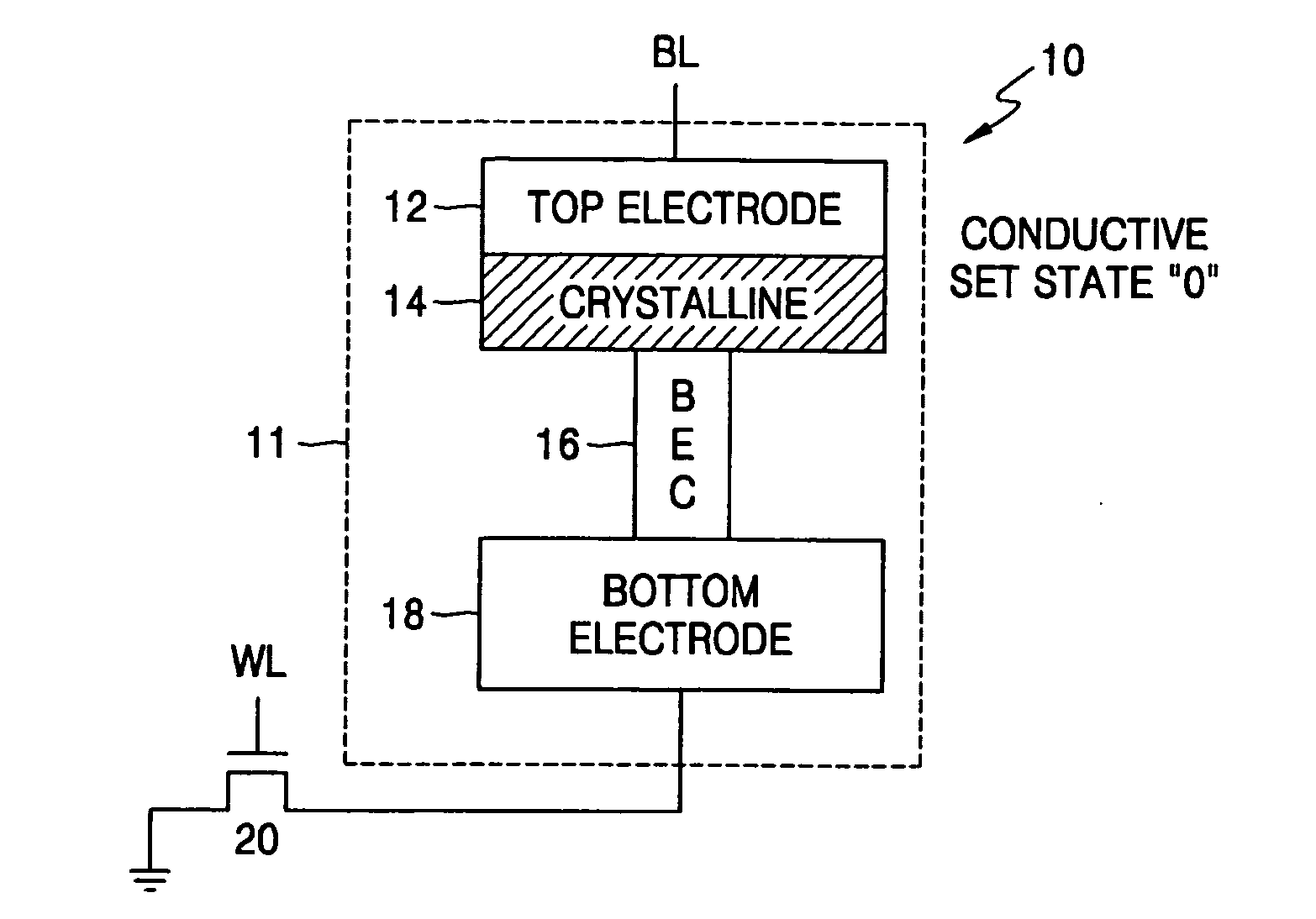
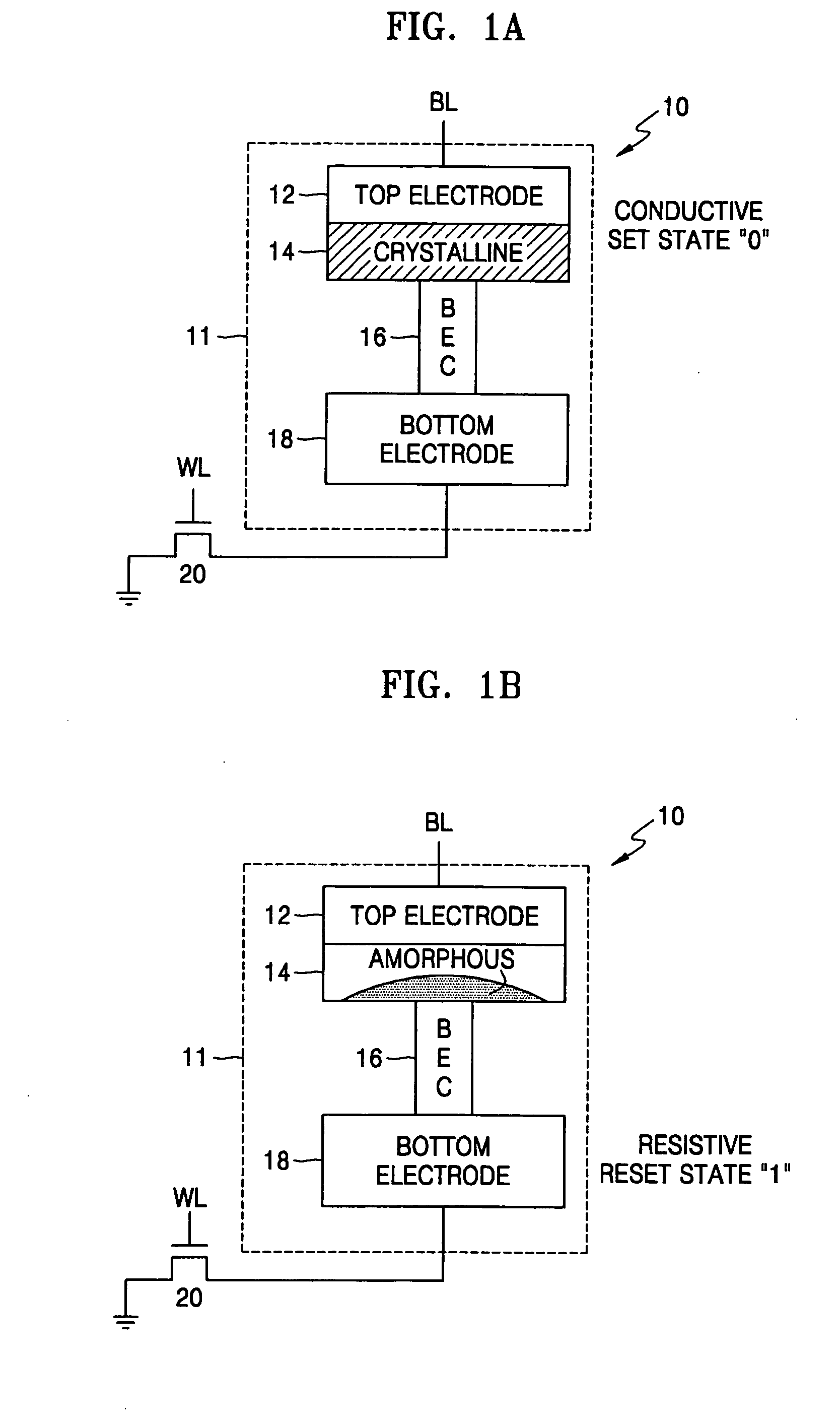
[0032] Reference is initially made to FIGS. 5A and 5B which respectively illustrate portions of memory cells 40 and 50 which, as a result of process variations, have bottom electrode contacts of different sizes.

[0033] In particular, FIG. 5A illustrates a first memory cell 40 having a top electrode 42, a phase-change material 44, and bottom electrode contact (BEC) 46. FIG. 5B illustrates a second memory cell 50 having a top electrode 52, a phase-change material 54, and a BEC 56. As is schematically shown, the BEC 56 of the second memory cell 50 is wider than the BEC 46 of the first memory cell 40.

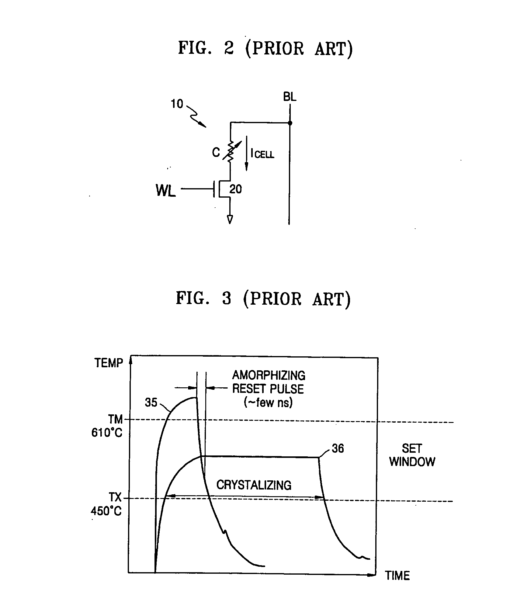
[0034] The ‘set’ current pulses and ‘reset’ current pulses are applied to the phase-change material 44 / 54 through the BECs 4...


PUM


Abstract

A method of programming a memory array including a plurality of memory cells is provided. The memory cells may include phase-change memory elements. In one aspect, the method includes applying in succession first through nth current pulses to each of the memory cells to be programmed to a first state (e.g., a crystalline state), where a current amplitude of the first through nth current pulses decreases with each successive pulse, and where a pulse duration of the first through nth current pulses increases with each successive pulse.

Description

BACKGROUND OF THE INVENTION [0001] 1. Field of the Invention [0002] The present invention generally relates to semiconductor memories, and more particularly, the present invention relates to method of programming a memory cell array. [0003] A claim of priority is made to Korean Patent Application No. 10-2005-0028086, filed Apr. 4, 2005, in the Korean Intellectual Property Office, the entirety of which is incorporated herein by reference. [0004] 2. Description of the Related Art [0005] A phase-change random access memory (PRAM), also known as an Ovonic Unified Memory (OUM), includes a phase-change material such as a chalcogenide alloy which is responsive to heat so as to be stably transformed between crystalline and amorphous states. Such a PRAM is disclosed, for example, in U.S. Pat. Nos. 6,487,113 and 6,480,438. [0006] The phase-change material of the PRAM exhibits a relatively low resistance in its crystalline state, and a relatively high resistance in its amorphous state. In conv...

Claims


Application Information

Patent Timeline
Patent Type & Authority Applications(United States)
IPC IPC(8): G11C11/00
CPCG11C13/0004G11C13/0069G11C2213/79G11C2013/0092G11C2013/0078G11C13/0038
Inventor KANG, SANG-BEOMKIM, DU-EUNGCHO, BAEK-HYUNGKIM, HYE-JIN
Owner SAMSUNG ELECTRONICS CO LTD
Why Eureka
Try Eureka