Pseudo SRAM

a random access memory and pseudo-semi-sram technology, applied in static storage, information storage, digital storage, etc., can solve the problems of degrading the operation performance of the conventional sram, and achieve the effect of preventing an increase in the access tim

Inactive Publication Date: 2006-10-05
SK HYNIX INC
View PDF9 Cites 24 Cited by
  • Summary
  • Abstract
  • Description
  • Claims
  • Application Information

AI Technical Summary

Benefits of technology

[0027] It is, therefore, an object of the present invention to provide a pseudo SRAM for preventing an increase of an access time due to a refresh operation.

Problems solved by technology

Accordingly, an operating performance of the conventional SRAM is degraded due to the increase of the read / write cycle time.

Method used


Image

  • Pseudo SRAM
  • Pseudo SRAM
  • Pseudo SRAM

Examples


Embodiment Construction

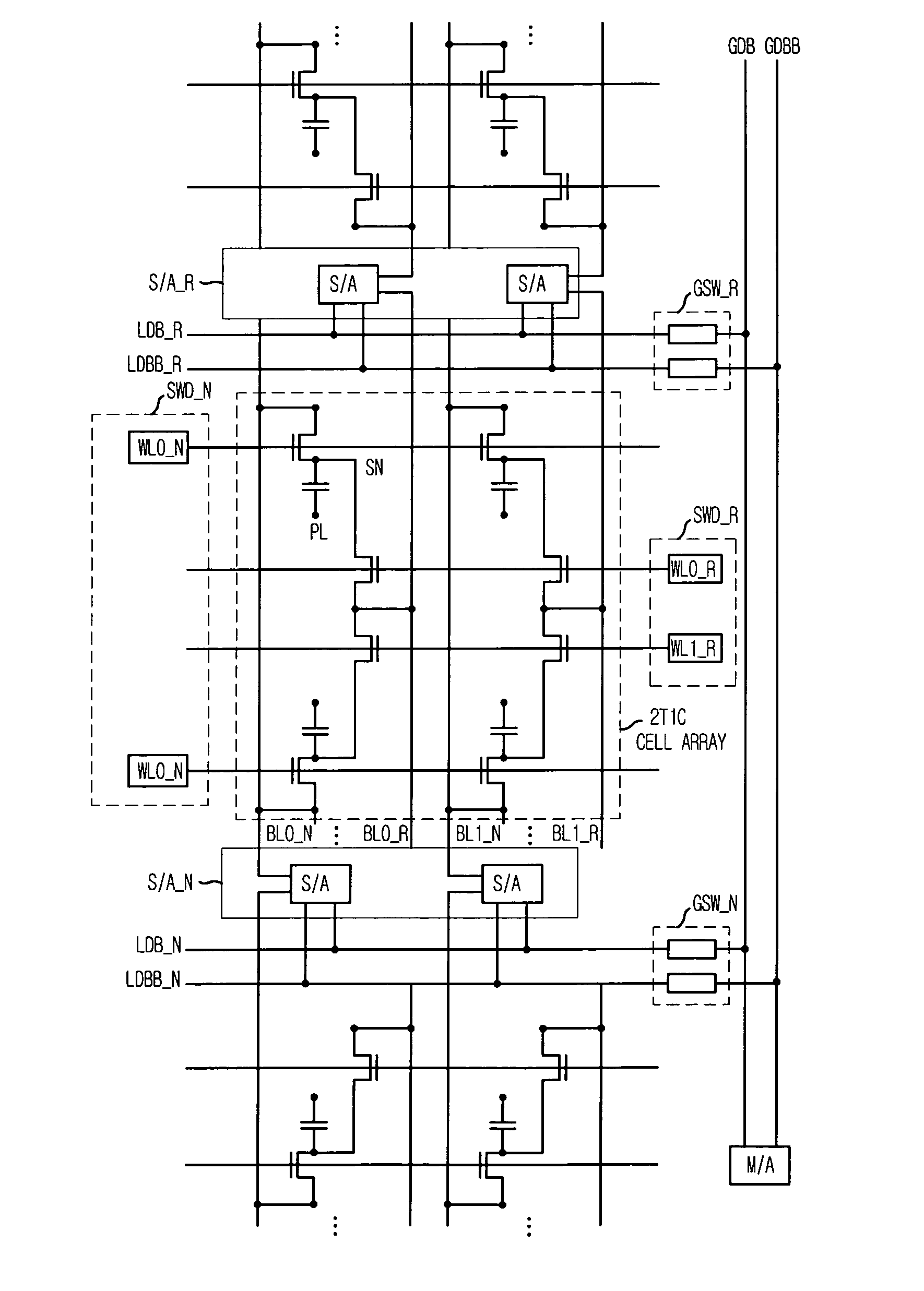
[0041] Hereinafter, a pseudo static random access memory (SRAM) in accordance with the present invention will be described in detail referring to the accompanying drawings.

[0042]FIG. 5 is a schematic circuit diagram showing a memory cell structure of a pseudo SRAM in accordance with a preferred embodiment of the present invention.

[0043] As shown, the memory cell of the pseudo SRAM includes a cell capacitor C, a normal accessing NMOS transistor T_N and a refresh accessing NMOS transistor T_R. A gate, a drain and a source of the normal accessing NMOS transistor T_N are respectively connected to a normal accessing word line WL0_N, a normal accessing bit line BL0_N and a storage node SN of the cell capacitor C. Similarly, a gate, a drain and a source of the refresh accessing NMOS transistor T_R are respectively connected to a refresh accessing word line WL0_R, a refresh accessing bit line BL0_R and the storage node SN of the cell capacitor C.

[0044] That is, the memory cell of the pse...


PUM


Abstract

A unit memory cell for use in a pseudo static random access memory (SRAM) includes a cell capacitor; a normal accessing transistor whose gate, drain and source are respectively connected to a normal accessing word line, a normal accessing bit line and a storage node of the cell capacitor; and a refresh accessing transistor whose gate, drain and source are respectively connected to a refresh accessing word line, a refresh accessing bit line and the storage node of the cell capacitor.

Description

FIELD OF INVENTION [0001] The present invention relates to a semiconductor memory device; and, more particularly, to a pseudo static random access memory. DESCRIPTION OF PRIOR ART [0002] A random access memory (RAM) is a semiconductor memory device for storing an input data in a memory cell array. Herein, each memory cell has an address to be selected. [0003] Generally, there are two different kinds of the RAM, i.e., one is a static random access memory (SRAM) and the other is a dynamic random access memory (DRAM). A memory cell of the SRAM has a static latching structure so that the data content of the memory cell can be maintained while a power is supplied to the SRAM. Herein, the memory cell of the SRAM includes four or six transistors (generally said to be a 4T or 6T structure). [0004] Meanwhile, a memory cell of the DRAM includes a single transistor and a single capacitor (generally said to be a 1T1C structure). Therefore, a conventional memory cell of the SRAM requires about 1...

Claims


Application Information

Patent Timeline
Patent Type & Authority Applications(United States)
IPC IPC(8): G11C7/00
CPCG11C11/40615G11C11/406
Inventor KANG, HEE-BOKAHN, JIN-HONG
Owner SK HYNIX INC
Why Eureka
Try Eureka