Detecting device and authentication device

a detection device and authentication technology, applied in the field of surface detection, can solve the problems of user cumbersome operation, detection device electric characteristics subject to fluctuations, etc., and achieve the effect of reducing the load of arithmetic processing

Active Publication Date: 2006-10-05
138 EAST LCD ADVANCEMENTS LTD
View PDF7 Cites 15 Cited by
  • Summary
  • Abstract
  • Description
  • Claims
  • Application Information

AI Technical Summary

Benefits of technology

[0006] An advantage of the invention is to provide a solution for performing detection evenly without the cumbersome operation of adjusting the reference signals, even though the characteristics of units of the detecting devices are subject to fluctuations.
[0007] According to an aspect of the intention, a detecting device includes: multiple sensors composed with a plurality of sensor circuits arrayed on a plane, each of which generates at least one detected signal that corresponds to a distance from a surface of an object; a selector circuit which selects each of the sensor circuits and outputs the detected signal from each of the sensor circuits; a storage which stores digital data of a reference value (for instance, a register 31 in the embodiments); a digital-to-analog converter circuit which generates a reference signal that corresponds to a level of the reference value from the digital data stored in the storage; a generation circuit (for instance, a comparator 35 in the embodiments) which generates, per each of the sensor circuits, in sequence, detected data according to a relationship of levels between the detected signal output from each of the sensor circuits selected by the selector circuit, and the reference signal generated by the digital-to-analog converter circuit; an arithmetic circuit which conducts a prescribed operation with a plurality of detected data sets generated by the generation circuit; a refresh circuit which refreshes the digital data stored in the storage, based on an operational value calculated by the arithmetic circuit; and an output circuit which conducts an output process, corresponding to the detected data generated by the generation circuit.
[0008] With this configuration, the digital data of the reference value is refreshed based on the detected data generated from the detected signals that each sensor circuit outputs. Hence, even though characteristics of the units, particularly that of the sensor circuit, the generation circuit, or the D/A conversion circuit are subject to fluctuation among different detecting devices, it is possible to perform the detection evenly and compensate the fluctuation thereof, without requiring a cumbersome operation such as adjustment of the reference value by the user.
[

Problems solved by technology

However, detecting devices are subject to fluctuations in the electric characteristics (particularly threshold voltages) of the switching element that constitutes part of the device, such as the sensor circuit that generates the detection signals and the comparator circuit that compares

Method used


Image

  • Detecting device and authentication device
  • Detecting device and authentication device
  • Detecting device and authentication device

Examples


first embodiment

[0029] First Embodiment

[0030] Structure of Detecting Device

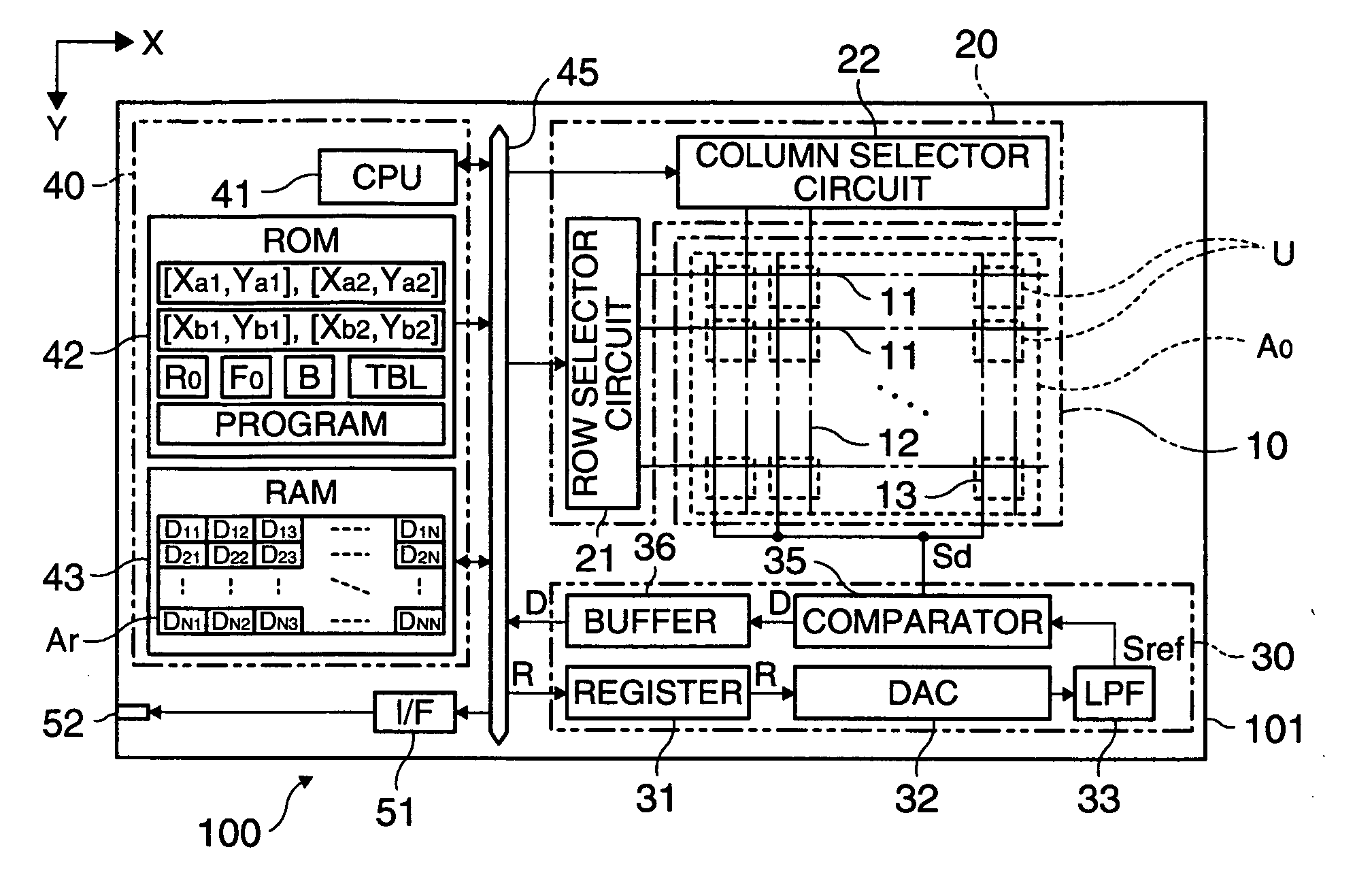
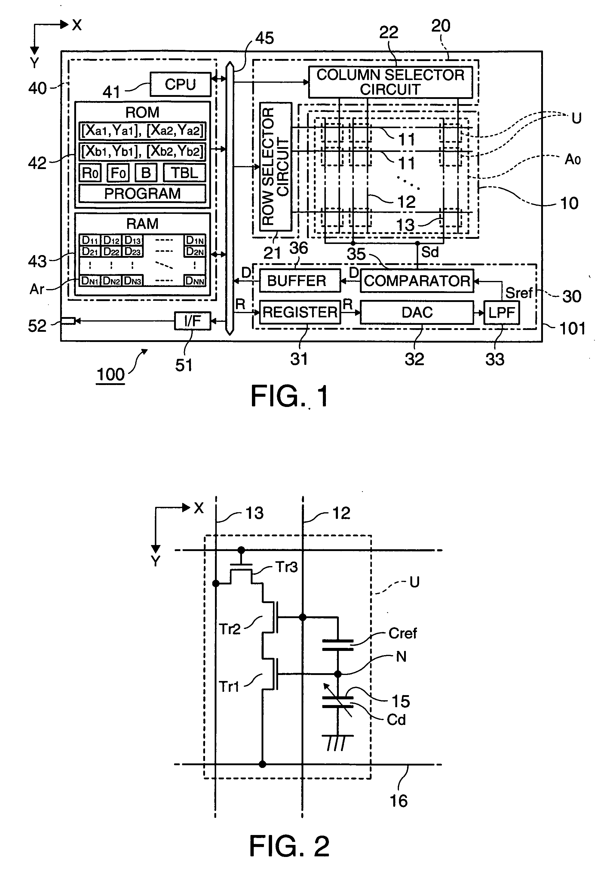
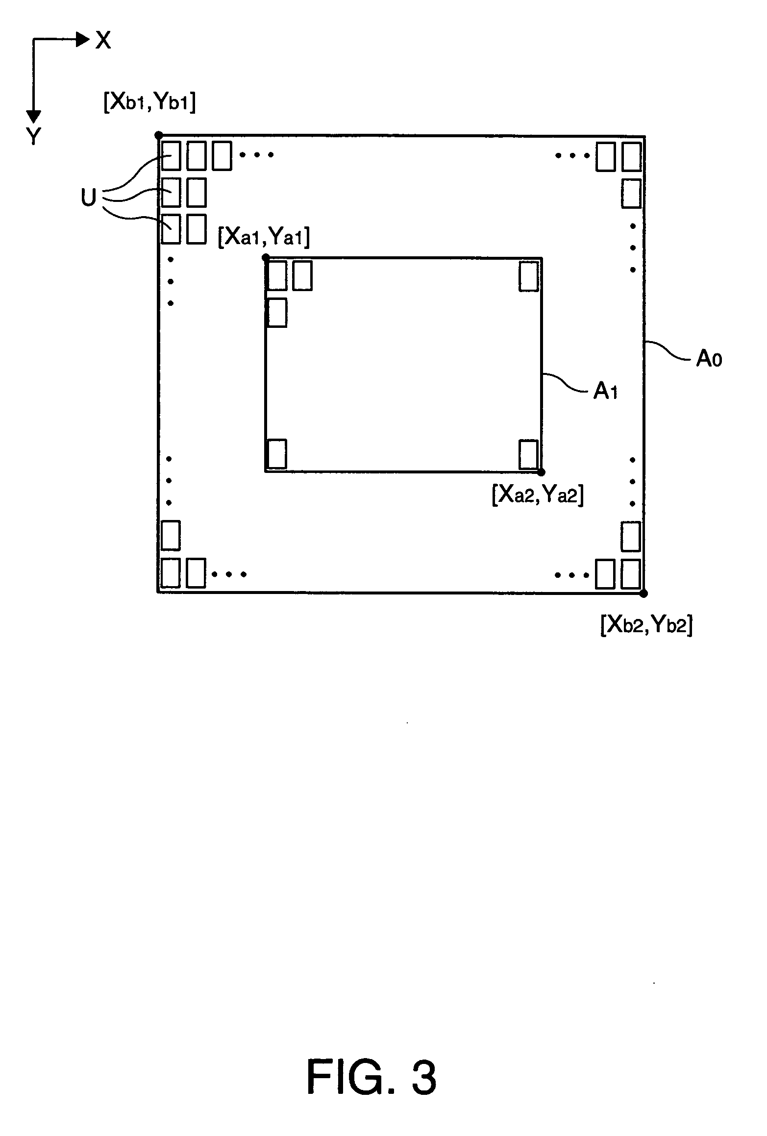
[0031]FIG. 1 is a block diagram illustrating the configuration of a detecting device according to this embodiment of the invention. A detecting device 100 detects a surface of an object close to or in contact with a surface exposed to the outside (hereafter referred to as “detecting surface”). As shown in FIG. 1, the detecting device 100 includes: multiple sensors 10 composed with a plurality of sensor circuits U arrayed in a matrix within a rectangular area A0 (hereafter “detection area”); a selector circuit 20 for activating each of the sensor circuits U in the multiple sensors 10; a detector circuit 30 that processes a signal Sd output from each of the sensor circuits U (hereafter “detected signal”); a control device 40 that controls the action of each unit in the detecting device 100; and an interface 51 for outputting the results of the detection by the detecting device 100 outward, and an output terminal 52 connected ...

second embodiment

[0062] Second Embodiment

[0063] A second embodiment according to the present invention will now be described. In the exemplary structure of the first embodiment, the pre-scan process for adjusting the reference signal Sref is performed as a different process from the main scan processing (in other words, the process to extract the detected data D that is an output target outward). In contrast, in this embodiment, the level of the reference signal Sref used in the next main scan process is adjusted, based on the detected data D extracted in the main scan process previous to that next main scan process. In this second embodiment, the same signs and numerals are used for the same elements as in the first embodiment, and the description thereof is omitted.

[0064] Operation of Detecting Device 100

[0065]FIG. 7 is a flow chart illustrating the steps of a program run by a CPU, according to this second embodiment of the invention. As shown in FIG. 7, the CPU 41 stores the initial value R0 sto...

first modified example

[0077] First Modified Example

[0078] The steps of the output process is not limited to the one in the exemplary structures of the embodiments, where the detected data D is output outward from the output terminal 52 in the output process of the step Sa14 in FIG. 4 or the step Sb6 in FIG. 7. Examples of the output process may include the steps described below.

[0079] First Exemplary Modification

[0080] As shown in FIG. 8, when the output process starts in the step Sa14 in FIG. 4 or in the step Sb6 in FIG. 7, the CPU 41 extracts parts that are characteristic when identifying the shape of the object's surface (hereafter referred to as “characteristic point”), based on the detected data D stored, at the start of the process, in the storage area Ar of the RAM 43 (step Sc1). This characteristic point is, for instance, a branching point or an end point of a fingerprint of human hand. Thereafter, the CPU 41 generates data which expresses the location of the characteristic points extracted in ...


PUM


Abstract

A detecting device includes: multiple sensors composed with a plurality of sensor circuits arrayed on a plane, each of which generates at least one detected signal that corresponds to a distance from a surface of an object; a selector circuit which selects each of the sensor circuits and outputs the detected signal from each of the sensor circuits; a storage which stores digital data of a reference value; a digital-to-analog converter circuit which generates a reference signal that corresponds to a level of the reference value from the digital data stored in the storage; a generation circuit which generates, per each of the sensor circuits, in sequence, detected data according to a relationship of levels between the detected signal output from each of the sensor circuits selected by the selector circuit, and the reference signal generated by the digital-to-analog converter circuit; an arithmetic circuit which conducts a prescribed operation with a plurality of detected data sets generated by the generation circuit; a refresh circuit which refreshes the digital data stored in the storage, based on an operational value calculated by the arithmetic circuit; and an output circuit which conducts an output process, corresponding to the detected data generated by the generation circuit.

Description

BACKGROUND [0001] 1. Technical Field [0002] The present invention relates to a technique for detecting the surface of an object with fine asperity. [0003] 2. Related Art [0004] Techniques for detecting a surface of an object with fine asperity, such as a human fingerprint, have been suggested. In JP-A-2004-317353, a detecting device in which multiple sensor circuits are arrayed in matrix along a contact surface of the object is disclosed. Here, each sensor circuit outputs a detection signal that is proportional to the distance between the contact surface and the object close thereto, or in contact therewith. With this structure, a comparator circuit is installed, and by analyzing the data output from the comparator circuit, the surface of the object is identified. Here, the comparator circuit outputs the data sets of two values, in accordance with a relationship between levels of a detection signal output from each sensor and a signal provided externally (hereafter referred to as “r...

Claims


Application Information

Patent Timeline
IPC IPC(8): G06K9/00
CPCG06K9/0002G06V40/1306
Inventor KARAKI, NOBUO
Owner 138 EAST LCD ADVANCEMENTS LTD
Why Eureka
Try Eureka